TAIYO YUDEN Solutions for Automotive UWB Design Challenges
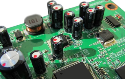
  RF Devices for Automotive UWB  Supporting the Evolution of Digital Keys  The adoption of UWB digital keys, which combine high-precision positioning with robust security, is accelerating rapidly. However, automotive UWB development faces three key technical challenges: compact footprint for high-density mounting, RF interference mitigation, and high reliability in harsh automotive environments.  TAIYO YUDEN provides RF devices featuring an ultra-compact form factor among the smallest in the industry and steep out-of-band noise attenuation. Enabled by our proprietary multilayer technology and rigorous automotive quality control, these solutions help resolve design challenges in next-generation mobility development.  Ultra-Compact Form Factor Among the Smallest in the Industry: 1608 Size (1.6 × 0.8 mm)  ・Achieves an industry-leading compact footprint using proprietary multilayer ceramic technology, contributing to high-density mounting in automotive modules and enhancing antenna layout flexibility.  RF Interference Suppression via Steep Attenuation Characteristics  ・Delivers both low insertion loss in the UWB band and steep out-of-band noise attenuation, ensuring stable operation in environments where multiple wireless systems coexist.  High Automotive Reliability Qualified to AEC-Q200  ・Supports automotive system design and qualification through high manufacturing quality backed by fully integrated domestic production and PPAP compliance.  Explore our full product lineup and detailed specifications on the Product Introduction Page.  Technical details are available in our white paper.  ▶Download White Paper  【Featured Automotive Solutions】  Explore our automotive components supporting the evolution of autonomous driving and ADAS.  Soft Termination MLCCs  Addresses reliability concerns such as board flexure cracking to ensure stable operation in harsh automotive environments.  Industry-leading High-Capacitance MLCCs for ADAS  3225 size / 220 µF among the highest capacitance products in the industry, contributing to advanced electronic system integration.  Conductive Polymer Hybrid Aluminum Electrolytic Capacitors (HTX-J/HVX-J Series)  Combines solid polymer and liquid electrolyte technologies to achieve high-voltage capability, high capacitance, and low ESR stability.
Key word:
Release time:2026-09-04 11:36 reading:177 Continue reading>>
TSMC: SoIC, CoWoS to Drive 50× Compute by 2029; Silicon Photonics to Top 50% of Transceiver Market by 2027
  TSMC is stepping up its technology roadmap to meet surging AI computing demand. According to TechNews, April Li, Global Head of AI and HPC Business Development at TSMC, said at SEMICON Taiwan 2026 that AI computing demand is growing fivefold annually, putting increasing pressure on compute capacity. In response, TSMC is integrating advanced process, 3DFabric, and silicon photonics into its HPC platform. Notably, the company expects SoIC and CoWoS integration to boost overall system computing performance to 50 times its 2024 level by 2029.  As the report indicates, Li said heterogeneous integration is the only way to push beyond current computing limits. TSMC plans N2P-on-N3P 3D integration in 2026, followed by A14-on-A14 in 2029, with interconnect pitch shrinking to 4.5 microns.  TSMC Advances COUPE and Silicon Photonics Design  TSMC is also continuing to advance its COUPE technology. According to TechNews, its 2–4-micron bonding pitch limits transmission loss at 112 Gbps to just 0.06 dB, compared with 1.38 dB for micro-bumps, helping reduce power consumption and latency to 10–20 nanoseconds.  As Mirror Daily indicates, TSMC’s self-developed COUPE platform uses TSMC-SoIC bonding technology to integrate electronic integrated circuits (EICs) with photonic integrated circuits (PICs), while supporting both grating couplers (GCs) and edge couplers (ECs). To further scale bandwidth, TSMC is pursuing two development paths. One will increase per-channel speeds from 200 Gbps to more than 400 Gbps while expanding channel counts from 16 to over 128, lifting total bandwidth from 3.2 Tbps to more than 12.8 Tbps. The other will expand wavelength-division multiplexing (WDM) from a single wavelength to 4, 8, 16, and beyond.  The company is also addressing testing and design challenges as CPO moves toward broader deployment. According to Mirror Daily, TSMC has enabled wafer-level optical testing for edge-coupled devices, allowing defective dies to be screened out before costly CPO assembly. TechNews adds that TSMC has introduced an optical PDK that enables electronic-photonic co-simulation to address key silicon photonics design challenges, while Mirror Media notes that the PDK supports Cadence and Synopsys tools to help accelerate product development.  Silicon Photonics Gains Ground as CPO Nears Mass Production  Beyond TSMC’s technology roadmap, silicon photonics is moving toward broader adoption and large-scale CPO deployment. As noted by Central News Agency, TSMC Vice President of Advanced Packaging Technology and Service K.C. Hsu said optical transceiver architectures are undergoing a structural shift, with silicon photonics expected to account for more than 50% of the optical transceiver market by 2027. CPO represents the next step, with some suppliers expected to begin mass production in the second half of 2026.  Hsu described optics as the “nervous system” of data centers as demand for high-speed connectivity grows. As noted by Central News Agency, he said optical transceiver sales rose 25% in 2025 and are expected to grow another 50% in 2026, while the high-end 100G-and-above market doubled in 2024 and expanded another 60% in 2025.  Hsu noted that Taiwan’s silicon foundry ecosystem is already capable of producing optical engines at scale and with high precision, while real-world data and market validation are helping ease longstanding concerns over CPO reliability. The bigger challenge to large-scale deployment now lies elsewhere in the supply chain, including lasers, optical fibers, fiber connectors, and product testing, he said, as reported by Central News Agency.
Key word:
Release time:2026-09-01 15:44 reading:199 Continue reading>>
Intel’s Advanced Packaging, Led by EMIB-T, Set to Hit Its Stride in 2029; DRAM Manufacturing Ruled Out
  Intel is gaining momentum in advanced packaging, with tech giants such as Google reportedly showing interest in its EMIB (Embedded Multi-die Interconnect Bridge) technology amid ongoing CoWoS supply constraints. Citing CFO David Zinsner’s remarks at Deutsche Bank’s 2026 Technology Conference on August 26, Investing.com reports that Intel expects advanced packaging revenue, led primarily by EMIB-T, to ramp in 2H27, become a steady contributor in 2028 and hit its stride in 2029.  Memory was another key topic at the conference, as AI reshapes the strategic importance of memory. Tom’s Hardware previously reported that Intel CEO Lip-Bu Tan had hinted at a potential return to the memory market. Zinsner, however, clarified that Intel has no plans to re-enter DRAM manufacturing, according to Investing.com.  Advanced Packaging Eyes 40% Gross Margin  Notably, Zinsner highlighted the scale and profitability potential of Intel’s expanding advanced packaging business. According to Investing.com, the opportunity could be worth several billion dollars per customer annually, with the business targeting around 40% gross and 30% operating margins. Its relatively low capital intensity versus front-end manufacturing could also support strong ROIC, he added.  In Zinsner’s words, Intel is “already eating our own dog food” with EMIB, indicating that the company is already deploying the technology in its own products. Building on EMIB, EMIB-T eliminates the need for an interposer, further enhancing the technology’s appeal and potential for broader adoption, he said.  According to Wccftech, Intel’s Clearwater Forest, or Xeon 6+, CPU features twelve EMIB tiles using 2.5D packaging. The design integrates three active base tiles with two I/O tiles and twelve compute tiles. The I/O tiles are built on Intel 7, while the active base tiles use Intel 3 and the compute chiplets are manufactured on Intel 18A, the report explains.  SK hynix Veteran’s Appointment Signals Intel’s Packaging Push  Lip-Bu Tan’s appointment of former SK hynix CEO Seok-Hee Lee as Intel Foundry’s executive vice president could fuel speculation that Intel is considering a return to memory manufacturing. However, according to an Investing.com transcript, Intel CFO David Zinsner instead pointed to Lee’s appointment as a strong vote of confidence in the growth potential of EMIB-T.  Bringing in an executive of Lee’s caliber to lead the business underscores Intel’s confidence in the opportunity and its long-term prospects, he added.  Intel Stays Out of DRAM Manufacturing  Notably, while Intel is developing memory-related technologies such as XHBM and Z-angle Memory (ZAM), Zinsner pushed back on speculation that the chipmaker plans to return to memory manufacturing.  According to Investing.com, he said Intel has no plans to resume DRAM production. Instead, Intel is working with three major memory players on AI-focused products and architectures designed to ease memory bottlenecks. Management emphasized that the company’s focus will remain on system-level memory solutions rather than manufacturing memory itself, according to the Investing.com transcript.
Key word:
Release time:2026-08-31 16:02 reading:209 Continue reading>>
Samsung’s 4nm GAIA Could Mark First PIM Commercialization in AI PCs, Mass Production as Early as 2027
Samsung is exploring a new approach to boost AI performance and efficiency on PCs. According to ZDNet, Samsung showcased its LPDDR5X-PIM paired with an edge AI accelerator SoC at Hot Chips. The company’s AI PC chipset under development, known as “GAIA,” is expected to incorporate LPDDR5X-PIM, which integrates computing capabilities directly into memory. This would mark the first integration of Processing-in-Memory (PIM) into an actual AI PC chipset. If GAIA reaches mass production, it could also become the first commercial application of PIM beyond the research and validation stage, the report notes.  GAIA is an AI accelerator for AI PCs being developed by Samsung Electronics’ System LSI division. Built on Samsung Foundry’s 4nm process, the chip is optimized for AI workloads. ZDNet adds that Samsung has reportedly provided GAIA prototypes to major PC makers, including Lenovo and HP, for performance validation, with mass production potentially beginning as early as next year.  LPDDR5X-PIM Delivers Up to 3.01x Higher Output in Testing  The key to the approach is reducing data movement. As the report explains, LPDDR5X-PIM adds computing capabilities directly to low-power LPDDR5X memory, allowing some data to be processed where it is stored rather than repeatedly transferred between memory and CPUs or GPUs. This can ease AI computing bottlenecks while reducing power consumption.  Samsung validated the SoC with both LPDDR5X and LPDDR5X-PIM, with PIM showing clear performance gains. LPDDR5X-PIM completed the test workload in 5.4 seconds versus 12.3 seconds for conventional LPDDR5X, a 2.28x improvement, while output jumped 3.01x from 27.0 to 81.3 per second, the report notes. ZDNet adds that Samsung previously said simulations showed up to 6.2x higher AI matrix-computation performance than conventional memory. These characteristics make LPDDR5X-PIM particularly suited to on-device AI, where laptops and smartphones face tight power and thermal limits.  GAIA Could Put PIM Commercialization to the Test  Samsung has been extending PIM technology across its memory portfolio, according to ZDNet. The company has introduced HBM-PIM for servers and integrated PIM with LPDDR for mobile applications. However, technical and ecosystem challenges have continued to limit its adoption in commercial products, the report adds. GAIA could therefore serve as a key test of PIM’s commercial potential. Sources cited by ZDNet note that if GAIA moves into mass production after customer validation in the AI PC market, PIM could evolve from a next-generation memory technology into a key solution for on-device AI.  Samsung is also lowering barriers to PIM commercialization. As noted by Seoul Economic Daily, its Address Alignment Mode (AAM) allows LPDDR5X-PIM to work with existing DRAM memory controllers, reducing the need for major system changes. The report adds that the first JEDEC specification for next-generation LPDDR6-PIM is nearing finalization, as Samsung looks to expand PIM from a proprietary solution into a standardized memory technology.  Meanwhile, SK hynix is also advancing PIM-based AI solutions. At CES 2026, the company showcased AiMX, an AI accelerator prototype built around its GDDR6-AiM PIM chip and designed for LLM workloads. The company also demonstrated other computational-memory technologies, including Compute-using-DRAM (CuD) and CMM-Ax.
Key word:
Release time:2026-08-27 13:46 reading:324 Continue reading>>
NOVOSENSE shares insights into automotive ultrasonic sensing at 2026 APEC 44th Automotive Dialogue
  NOVOSENSE shared its latest insights into automotive AK2 ultrasonic radar sensor ICs at the 44th Automotive Dialogue of the Asia-Pacific Economic Cooperation, or APEC, held in Dalian, Liaoning province, China, from Aug 19 to 21.  The meeting brought together representatives from government departments, industry associations and companies across APEC economies. Discussions focused on automotive market, policy and industry trends in the Asia-Pacific region, resilient and transparent automotive supply chains, the development of the hydrogen vehicle industry, and opportunities and challenges in advanced vehicle technologies.  Liangfan Wang, technical marketing lead for the signal chain product line at NOVOSENSE, delivered a presentation on technology trends and practical solutions for AK2 ultrasonic radar sensor ICs, exchanging ideas with participants on the challenges and opportunities in automotive intelligent sensing.  Shift toward digital architectures  Automotive ultrasonic radar is moving from analog to digital architectures. Compared with the conventional AK1 analog architecture, AK2 uses digitally encoded modulation and echo signal processing to improve detection range, measurement accuracy and resistance to interference.  Its interface has also evolved from point-to-point connections to a shared bus that supports coordinated operation among multiple sensors. AK2 ultrasonic radar has been applied in ultrasonic parking assist, automatic parking assist and automated valet parking systems.  Development of multidimensional sensing  Automotive ultrasonic sensing is expanding from 1D and 2D ranging toward 3D and 4D sensing. Its applications are also extending to low-speed automatic emergency braking, obstacle-type detection, road-surface classification and minor-impact detection.  The technology continues to provide advantages in short-range sensing while working alongside millimeter-wave radar, ultra-wideband technology and cameras.  Bumper-level sensing cycles are being reduced to less than 100 milliseconds, allowing vehicles to detect obstacles earlier and improving the efficiency of automated valet parking. This requires sensor ICs to provide stronger coordination among multiple transmit and receive channels, as well as greater resistance to interference.  Further improvements are also required for object classification, road-surface recognition, sensor contamination detection and near-field blind-zone reduction. These functions require access to raw sensing data at different stages of signal processing.  At the system level, MCU-less designs, two-wire DSI3 connectivity and direct-drive architectures can help reduce component and wiring-harness costs. The DSI3 architecture carries power and communication over the same pair of wires, while the direct-drive architecture removes the need for an external transformer.  Flexible encoding reduces sensing time  NOVOSENSE uses an arbitrary frequency pattern generator to provide fixed-frequency transmission, linear and nonlinear frequency encoding, and combined frequency-shift keying and chirp encoding.  The solution supports multiple transmit and receive operation to improve resistance to interference. A bumper scan can be completed within two scanning cycles.  Raw-data access extends the sensing range  NOVOSENSE provides a configurable data-upload path with selectable decimation ratios ranging from 1× to 16×. Data can be compressed by the MCU before being uploaded through the DSI3 interface.  Available data includes ADC raw data within a 2-millisecond window, post-mixing in-phase and quadrature data, and envelope data captured before and after an event.  A time-varying low-noise amplifier automatically switches gain to reduce near-field saturation. The solution covers detection distances ranging from about 10 centimeters to 6.5 meters.  DSI3 supports cross-brand interoperability  NOVOSENSE has developed a cross-brand interoperability architecture based on the standard DSI3 protocol. It supports combinations of NOVOSENSE devices and other industry-standard DSI3 devices, as well as point-to-point, parallel and daisy-chain configurations.  The NSUC1800 supports vendor-defined Command and Response Mode commands, while the NSUC1802 provides a DSI3 buffer of 2 kilobytes per channel. The two products address different requirements for functional expansion and flexible data access.  About the APEC Automotive Dialogue  Established in 1998, the APEC Automotive Dialogue provides a regular communication platform for government authorities and automotive industry representatives from APEC economies. It promotes exchanges and cooperation in areas including development strategies, standards and regulations, and technological innovation.
Key word:
Release time:2026-08-26 14:03 reading:383 Continue reading>>
NVIDIA Reportedly Eyes More Than 15% Price Hikes for Vera Rubin, Grace Blackwell Servers in Early 2027
  NVIDIA is reportedly moving to raise prices across its AI server ecosystem. According to Bloomberg, sources say prices for servers powered by NVIDIA’s AI chips will increase by more than 15% for some of its biggest customers. The hikes will apply to systems shipped early next year, including those featuring NVIDIA’s flagship Vera Rubin and Grace Blackwell chips, with the size of the increase varying by chip generation and memory configuration.  Server manufacturers that build systems under contract for major data center operators, including Microsoft, Alphabet’s Google, and Oracle, have reportedly informed customers of the upcoming increases. The move comes as memory supply remains a key consideration for AI systems. Wccftech notes that analysts believe NVIDIA may have secured multi-year agreements with SK hynix and Micron for HBM and DRAM supplies.  The higher prices are also raising concerns about rising costs for AI data center development and operations worldwide. Chosun Ilbo, citing The Information, notes that the increases could add at least US$5 billion (approximately KRW 7 trillion) to the cost of building a 1-gigawatt (GW) AI data center.  Memory Supply Emerges as Key AI Chip Pricing Factor  Meanwhile, Hankyung notes that higher NVIDIA AI chip prices could weigh on the broader AI data center ecosystem, potentially slowing demand and bringing the rise in memory prices to a halt.  Analysts cited by Hankyung say NVIDIA’s decision to pass higher costs on to customers highlights the growing influence of memory suppliers. With memory supply increasingly affecting both AI chip production volumes and pricing, its role in overall system costs is also expanding. Morgan Stanley notes that GPUs once accounted for more than 80% of AI server costs, but their share has fallen to roughly half that level in next-generation systems as memory-related costs rise rapidly.  According to TrendForce, server DRAM contract prices are expected to rise 13–18% quarter-over-quarter in 3Q26. With the market remaining undersupplied, memory suppliers may continue revising quotations upward throughout the rest of the quarter. Overall, TrendForce expects server DRAM contract prices to continue rising each quarter from the second half of 2026 through the second half of 2027, although the pace of increases is likely to moderate.
Key word:
Release time:2026-08-25 15:11 reading:335 Continue reading>>
SK hynix Reportedly Builds Silicon Valley HBM Team to Boost Customer Co-Design With U.S. Big Tech
  SK hynix is reportedly strengthening its HBM co-design capabilities in Silicon Valley as it deepens collaboration with global Big Tech customers. According to NewsPim, sources say SK hynix America operates an HBM Architect Design Team in San Jose, California, working directly with major U.S. customers on base-die design for HBM and 3D-stacked DRAM. The team develops next-generation HBM architectures around customer requirements, going beyond local technical support to collaborate throughout product development.  Notably, NewsPim adds that SK hynix is expanding the team, offering annual salaries of US$150,000–US$260,000. The company is seeking experience in DRAM and HBM architecture, full-custom and digital co-design, power delivery network (PDN) analysis, and logic foundry design, with experience in 1x-nanometer DRAM and foundry nodes of 3nm or below preferred. Developing advanced, customer-tailored HBM architectures for future products is among the team’s core responsibilities, the report notes.  The San Jose location also supports this strategy. As NewsPim notes, NVIDIA and AMD are headquartered in nearby Santa Clara, while Broadcom has operations in San Jose. Positioning HBM engineers near these major AI chip design hubs allows SK hynix to work directly with customers on next-generation products and quickly relay their requirements to development teams in South Korea.  SK hynix is already deepening such collaboration with NVIDIA. Chosun Ilbo notes that the two companies are jointly developing next-generation memory for AI factories, expanding their partnership beyond supplying existing HBM toward developing advanced memory aligned with NVIDIA’s next-generation roadmap.  Customer Co-Design Reshapes HBM Competition  Customer co-design is expected to become even more important with HBM4 and future generations. As NewsPim notes, increasingly diverse AI accelerator architectures are driving different requirements for HBM capacity, bandwidth, and power, making early co-optimization of AI chips and memory increasingly important.  This is also reshaping HBM competition. Memory suppliers that participate early in customers’ next-generation AI chip development can incorporate specific requirements into their designs, while co-developed HBM may raise barriers for rivals seeking to enter the same supply chain later. As the report points out, such collaboration is becoming increasingly important for securing next-generation HBM orders.  The trend extends beyond SK hynix. Seoul Economic Daily notes that Samsung is recruiting base-die designers as customer-specific optimization for AI accelerator vendors becomes increasingly important with HBM4. The company is also hiring application engineers to evaluate HBM on AI accelerator systems and support key customer qualifications, with the aim of shortening the certification process.
Key word:
Release time:2026-08-20 11:44 reading:375 Continue reading>>
TSMC Arizona Profit Soars 663% YoY in 1H26; U.S. Earnings Pull Back 8.2% QoQ in 2Q as Depreciation Bites
  As TSMC’s Arizona fabs ramp up to meet strong demand from NVIDIA and other Big Tech customers, the U.S. unit has overtaken TSMC Nanjing as the foundry giant’s most profitable overseas subsidiary. Citing TSMC’s 1H26 interim report, Commercial Times and the Economic Daily News report that TSMC Arizona posted a record NT$36.066 billion profit in 1H26, up 662.8% YoY.  As TSMC’s overseas footprint moves into a profit-harvesting phase, its four major manufacturing subsidiaries generated a combined NT$58.529 billion in 1H26, up 215.4% YoY. TSMC Arizona alone contributed more than 60% of the total, underscoring its growing weight in TSMC’s overseas earnings mix, as highlighted by the Economic Daily News.  Arizona Fab Profit Pulls Back QoQ as Depreciation Pressure Mounts  However, the Arizona profit surge showed signs of moderating in Q2. Its profit slipped 8.2% QoQ to NT$17.259 billion, even as it remained up a hefty 307.8% YoY, according to the Economic Daily News. Commercial Times further notes that TSMC recognized about NT$14.603 billion in investment income from its U.S. fab in the second quarter, down 13.6% from NT$16.909 billion in the first quarter.  Analysts cited by Commercial Times pointed out that as construction of subsequent fabs accelerates, higher depreciation and amortization expenses could put pressure on profitability.  TSMC has already warned that the overseas fab ramp-up will weigh on margins. CFO Wendell Huang said at the July earnings call that overseas expansion is expected to dilute gross margin by 2–3 percentage points in the early stages, widening to 3–4 points as the fabs mature.  As highlighted by Commercial Times, TSMC’s first Arizona fab entered 4nm mass production in 4Q24, while the second, focused on 3nm, is slated to ramp in 2H27. With the latest $100 billion investment, total planned U.S. investment has reached $265 billion, with the Arizona site ultimately expected to house 10 fabs and two advanced packaging facilities, according to MoneyDJ. How this aggressive expansion will impact profitability remains a key watchpoint.  Nanjing, JASM Profits Ease as Overseas Earnings Face New Tests  TSMC’s Nanjing fab remained a key profit driver, posting NT$14.978 billion in 1H26 and ranking second among its four major overseas operations. However, Q2 profit edged down to NT$7.389 billion from NT$7.589 billion in Q1, according to Economic Daily.  Meanwhile, JASM’s earnings also cooled slightly in Q2. As noted by Commercial Times, the Japan subsidiary, 73%-owned by TSMC, turned profitable this year after posting a loss in 2025, earning NT$951 million in Q1 and NT$727 million in Q2.  The bigger question now is whether JASM can keep that momentum after the July 7.1-magnitude Kumamoto earthquake. Commercial Times notes. The fab has resumed normal production and passed structural safety checks, but equipment requalification, calibration and wafer losses could reportedly weigh on Q3 results.
Key word:
Release time:2026-08-18 11:25 reading:268 Continue reading>>
Micron Flags HBM4E as Start of Custom HBM Era; HBM Market Could Tilt Toward Dual-or-Single Suppliers
  Memory giants are increasingly turning to custom HBM as the next growth engine. At the KeyBanc Technology Leadership Forum 2026, Micron EVP Sumit Sadana, according to Investing.com, said the shift toward custom HBM will begin with HBM4E, with the company planning to work with customers on custom SKUs.  More notably, Sadana pointed to a potential shake-up in the HBM supplier landscape. Given the time, R&D and cost involved in HBM design and qualification, he said customers are unlikely to work with all three HBM suppliers across every project—potentially pushing the market toward a two-supplier or even single-source model, as noted in the Investng.com transcript.  That would mark a significant shift from today’s landscape, where SK hynix, Samsung and Micron have all begun supplying HBM4 to NVIDIA’s Vera Rubin.  HBM’s Growing Capacity Squeeze  In the Investing.com transcript, Micron EVP Sumit Sadana highlighted the power-efficiency edge of its HBM3E, which consumes 30% less power than the next-best offering while remaining in high-volume production. But HBM’s rapid ramp-up is also putting increasing pressure on conventional DRAM supply, further tightening an already constrained memory market.  Sadana reiterated the 3:1 HBM-to-DDR trade-off: producing 100 bits of HBM3E effectively requires sacrificing around 300 bits of DDR supply. The capacity squeeze is set to intensify with newer HBM generations — as Micron moves through HBM4 and into HBM4E, that ratio is expected to worsen to nearly 4:1.  Custom HBM Gains Momentum Among Memory Leaders  At the J.P. Morgan 54th Annual Global Technology, Media and Communications Conference in May, Micron’s Global Operations EVP Manish Bhatia, via STOCK Analysis transcript, already flagged the company’s custom HBM roadmap. According to Bhatia, the company’s first HBM4E will be a JEDEC-standard product, with ramp-up scheduled for 2027.  While Micron is still using 1-beta DRAM for HBM4, Bhatia said the company is expected to transition to 1-gamma DRAM in the HBM4E era. He also confirmed that the logic dies for both standard and custom HBM4E are expected to be manufactured by TSMC.  Micron is not alone in stepping up its custom HBM push. News1 reports that SK hynix has launched a recruitment drive for its “Next Memory Strategy” division through its monthly “Highway” career hiring program. The team will focus on developing customer-tailored memory solutions and identifying new memory business opportunities, the report suggests.  That strategy is already taking shape through SK hynix’s “One Team” model. As reported by Sisa Week, unlike Samsung’s integrated, in-house approach, SK hynix’s approach brings together itself, NVIDIA, and TSMC, with NVIDIA defining the HBM requirements for its GPUs, SK hynix handling memory stacking, and TSMC manufacturing the logic die and handling packaging.
Key word:
Release time:2026-08-13 13:08 reading:278 Continue reading>>
SK hynix’s Chongqing Sale Plan Signals a Global Production Reset, Not a China Exit—Or Full Ownership of Every Site
  Coinciding with SK hynix’s KRW 54.3 trillion investment in the Yongin Y2 and Cheongju M17 fabs, Bloomberg reports that the memory giant is considering bringing in external investors or selling a stake in its Chongqing semiconductor packaging plant, valued at around KRW 4 trillion ($3 billion). The move has fueled speculation that SK hynix could be reshaping its China operations alongside its massive domestic investment.  SK hynix, however, has yet to confirm any deal. According to Newsis, the company said on Aug. 10, in response to a Korea Exchange inquiry, that it is “reviewing various measures to strengthen the competitiveness of its packaging business,” but “nothing has been finalized.”  As noted by S Journal, it would therefore be premature to view the move as a China exit. SK hynix continues to produce DRAM in Wuxi, while Dalian—acquired through Intel’s NAND and SSD business—remains a key NAND flash front-end hub. China is still expected to account for around 30–35% of SK hynix’s DRAM capacity and 35–40% of its NAND capacity in 2026, according to TrendForce.  Chongqing Plant: From $1B Investment to $3B Valuation  S Journal further explains that SK hynix’s Chongqing plant, which began mass production in July 2014, is a major back-end processing hub in China. As suggested by the report, the plant was built as SK hynix expanded its China production network to meet the growing global NAND flash market.  According to Chinese tech outlet TechPlus, cited by Sohu, SK hynix’s Chongqing facility employs around 3,000 people, with reported investment of more than $1 billion but less than $1.5 billion. At the roughly $3 billion valuation now under discussion, SK hynix could be looking at a sale price roughly two to three times its reported investment, underscoring the potentially substantial value uplift of the asset.  As reported by Bloomberg, Chinese investment funds and local semiconductor companies are among the potential buyers, while SK hynix is also weighing a partial stake sale that would allow it to retain a minority interest. However, Green Economy News notes that the talks are still at an early stage, with no deal or sale structure finalized.  SK hynix Weighs Reshaping Its China Packaging Footprint  More broadly, the potential move could reflect SK hynix’s efforts to reduce geopolitical exposure in China while shifting more of its AI memory supply chain toward Korea and the U.S., where customer access is stronger, Green Economy News reports. An industry source cited by the outlet said the company’s China strategy remains fluid, but the broader trend toward Korean front-end production and U.S.-based advanced packaging is likely to gain momentum.  As noted by Green Economy News, the shift is already visible in SK hynix’s packaging buildout across Korea and the U.S. The company is investing $3.87 billion (KRW 5.2 trillion) in West Lafayette, Indiana, to build an advanced packaging plant for AI memory, including HBM, with mass production targeted for 2H28. In Korea, it is also building the P&T7 advanced packaging plant at its Cheongju campus, slated to begin operations in 2028.  SK hynix Rewires Its Production Map  On Aug. 7, SK hynix’s board approved KRW 54.3 trillion in investment through 2031 for the Y2 fab at the Yongin semiconductor cluster and the M17 fab in Cheongju. The move underscores a broader shift: while reassessing the ownership structure of its existing Chinese back-end assets, SK hynix is committing more than KRW 50 trillion to next-generation capacity in Korea, as highlighted by S Journal.  More broadly, the strategy suggests SK hynix is rethinking where to own, where to invest, and what role each production site should play in its future technology roadmap, rather than simply maintaining full ownership of every facility, according to S Journal. As suggested by the report, in Korea, the company is expanding next-generation DRAM, HBM, and NAND capacity centered on Yongin and Cheongju, while strengthening the integration of front-end production and advanced packaging in Cheongju. Meanwhile, in the U.S., it is building advanced packaging and R&D capabilities for next-generation HBM.
Key word:
Release time:2026-08-11 14:20 reading:458 Continue reading>>

Turn to

/ 252

  • Week of hot material
  • Material in short supply seckilling
model brand Quote
MC33074DR2G onsemi
RB751G-40T2R ROHM Semiconductor
BD71847AMWV-E2 ROHM Semiconductor
TL431ACLPR Texas Instruments
CDZVT2R20B ROHM Semiconductor
model brand To snap up
IPZ40N04S5L4R8ATMA1 Infineon Technologies
ESR03EZPJ151 ROHM Semiconductor
BU33JA2MNVX-CTL ROHM Semiconductor
STM32F429IGT6 STMicroelectronics
BP3621 ROHM Semiconductor
TPS63050YFFR Texas Instruments
Hot labels
ROHM
IC
Averlogic
Intel
Samsung
IoT
AI
Sensor
Chip
About us

Qr code of ameya360 official account

Identify TWO-DIMENSIONAL code, you can pay attention to

AMEYA360 mall (www.ameya360.com) was launched in 2011. Now there are more than 3,500 high-quality suppliers, including 6 million product model data, and more than 1 million component stocks for purchase. Products cover MCU+ memory + power chip +IGBT+MOS tube + op amp + RF Bluetooth + sensor + resistor capacitance inductor + connector and other fields. main business of platform covers spot sales of electronic components, BOM distribution and product supporting materials, providing one-stop purchasing and sales services for our customers.

Please enter the verification code in the image below:

verification code