Samsung Reportedly Developing 4nm GAIA AI PC Chip; Mass Production Targeted as Early as 2027
  Samsung is reportedly preparing to enter the AI PC chip market. According to Hankyung, industry sources say Samsung Electronics’ System LSI Business under the Device Solutions (DS) Division is developing GAIA, a 4nm AI accelerator for AI PCs. Prototype chips have reportedly already been provided to major customers, including Lenovo and HP, for performance validation, with mass production targeted as early as 2027.  Samsung plans to pair GAIA with processing-in-memory (PIM), a next-generation DRAM technology that performs computations directly within memory, as the report indicates. Unlike traditional PC processors, GAIA is designed specifically for AI workloads, with an optimized NPU architecture aimed at efficiently handling generative AI tasks.  The reported move follows Samsung’s earlier attempt to enter the PC chip market 14 years ago with an Exynos application processor that powered Samsung Chromebooks in 2012. However, it failed to break Intel’s dominance and withdrew from the business roughly two years later.  AI PC Chip Competition Intensifies  Samsung’s reported move positions it alongside a growing number of companies targeting the AI PC market. The report says the segment remains in its early stages and has yet to produce a dominant player as the AI agent era begins to emerge. Companies including NVIDIA, Qualcomm, Intel, and Huawei are already competing in the space. NVIDIA unveiled its next-generation RTX Spark AI PC chip in May, while Qualcomm first introduced the Snapdragon X Elite in 2023 before expanding its lineup with the entry-level Snapdragon C.  EBN News says Samsung Electronics aims to differentiate itself by leveraging its leadership in memory alongside the AI chip design expertise gained from developing smartphone APs and mobile NPUs. Industry observers believe that combining AI accelerators with processing-in-memory (PIM) technology could enhance both AI processing performance and power efficiency.  Industry observers cited by Hankyung say the success of Samsung’s AI PC chip initiative will depend largely on its ability to secure major customers and bring the product to market. If the company achieves mass production and builds a stable supply chain, the business could emerge as a key growth driver, helping the System LSI Business address its long-standing structural losses.  Despite the growth opportunity, Samsung’s expansion into the AI accelerator market may also present strategic challenges. Hankyung notes that companies including NVIDIA and Qualcomm, which Samsung is expected to compete against in the AI PC market, are also among Samsung Foundry’s key customers.
Key word:
Release time:2026-07-13 13:53 reading:312 Continue reading>>
Largan Expands CPO Push, Plans September Fiber Array <span style='color:red'>Pi</span>lot Line, Eyes 2027 Revenue Contribution
  Taiwan’s Largan Precision, a key optical lens supplier in Apple’s supply chain, is expanding into CPO. According to Liberty Times, Chairman Adam Lin said after the company’s shareholders’ meeting today that Largan plans to establish an automated pilot production line for its fiber array (FA) products in September and may invite a potential major customer to visit the facility.  Lin said the company has developed a proprietary technology that enables conventional V-grooves and optical fibers to be assembled into high-precision FA products. He noted that tolerance stack-up between V-grooves and optical fibers has been a key challenge for the industry, often forcing competitors to rely on the highest-precision V-grooves and optical fibers to achieve the required accuracy. Largan, however, can use less-than-perfect components to produce FA products with precision below 0.3 microns, outperforming the industry’s typical range of 0.5 to 0.8 microns, the report highlights.  Largan made its first appearance at Computex this year, showcasing CPO-related solutions and expanding into optical components such as FAUs (fiber array units) and MLAs (microlens arrays). The move is widely viewed as an important signal that the company is seeking new high-margin growth drivers beyond its core smartphone lens business, as noted by China Times.  The company’s investment in fiber arrays aligns with growing demand for CPO technologies. TrendForce forecasts that co-packaged optics (CPOs) will steadily increase their share of optical communication modules in AI data centers, with penetration potentially reaching 35% by 2030.  Largan Sees Multi-Row FAs as Next Growth Driver  FAUs (fiber array units) combine FAs with components such as microlens arrays (MLAs) and prism microlens arrays (PMLAs). According to Liberty Times, Lin expects single-row products to remain the industry’s primary source of demand through 2028. Over the next three to four years, however, rising computing requirements are expected to drive a gradual shift toward two-row, four-row, and eventually eight-row configurations, the report notes. Lin said this transition would play to Largan’s strengths, citing the company’s multilayer stacking and high-precision technologies as key differentiators.  Largan Eyes 2027 FA Revenue as Qualification Process Advances  Looking ahead, Lin said FA products could begin contributing to revenue in 2027 if Largan successfully completes customer qualification, the Liberty Times report notes. However, because the products have yet to enter mass production, the company is not currently able to estimate yields or gross margins. Meanwhile, preparations for low-volume production are expected to take about six months to one year. Lin said the production line will be highly automated to improve process precision and manufacturing capacity while reducing reliance on labor-intensive production.
Key word:
Release time:2026-06-10 10:29 reading:752 Continue reading>>
Samsung Starts Shipping Industry-First HBM4E Samples 3 Months After HBM4 Ramp; Performance Up 20%+
  Just months after rolling out HBM4 shipments in early 2026, Samsung has begun providing samples of the industry’s first 12-layer HBM4E to major global partners, according to the company’s latest press release.  Given that HBM4 shares the same 1c DRAM process and 4nm base die architecture as HBM4E, and is already in mass production, industry observers suggest the newly shipped HBM4E samples are also well positioned to transition into mass production. Samsung adds that it plans to proceed with HBM4E mass production in line with client-specific timelines.  Meanwhile, Samsung is also expanding mass production and supply of HBM4, which became the world’s first HBM4 to enter mass production and shipment in February. In December last year, Samsung’s HBM4 received top-tier evaluation after demonstrating an industry-leading 11.7Gbps speed in System-in-Package (SiP) testing, the final certification stage, the company adds.  According to News1, the latest development makes Samsung the first to supply HBM4E. Industry observers cited by the report also noted that starting from HBM4, customer-specific design flexibility and stable large-scale supply capabilities will become even more critical. Against this backdrop, Samsung’s integrated strengths across memory, foundry, and advanced packaging are expected to stand out even more clearly, the report adds.  HBM4E Upgrade with 20% Performance Boost, 30% Higher Capacity  In terms of performance, Samsung notes that HBM4E marks a notable upgrade over the previous generation, offering a stable 14Gbps pin speed that can scale up to 16Gbps for more demanding AI workloads. Compared with HBM4, the new memory delivers over 20% higher performance and reaches bandwidth of up to 3.6TB/s per stack, significantly improving compute efficiency for large language models (LLMs) and next-generation AI systems.  Additionally, Samsung’s 12-layer HBM4E is currently offered in a 48GB capacity, which is more than 30% higher than the previous generation. The company plans to expand the lineup to include 32GB (8-layer) and 64GB (16-layer) variants to better align with diverse customer requirements as well.  From an efficiency standpoint, Samsung highlights that advanced low-power design techniques and an optimized packaging architecture have improved energy efficiency by 16% while reducing thermal resistance by more than 14% compared with the previous generation.  HBM4E Progress Among Rivals  Meanwhile, progress from SK hynix and Micron in HBM4E has come under closer market scrutiny following Samsung’s advances. According to Yonhap News Agency, SK hynix had initially planned to begin HBM4E sample shipments in the second half of this year, but recent reports indicate smoother-than-expected development progress, bringing forward its timeline.  On the other hand, Micron said its first HBM4E product will follow JEDEC standards, with mass production ramp-up targeted for 2027, according to STOCK Analysis.
Key word:
Release time:2026-05-29 10:18 reading:948 Continue reading>>
Samsung Reportedly Develops Mobile HBM Packaging With Copper <span style='color:red'>Pi</span>llars, Bandwidth Up 15%–30%
  Samsung Electronics is reportedly developing a next-generation HBM packaging technology aimed at bringing high-performance on-device AI to mobile devices. According to ETNews, sources say the company is working on a “Multi Stacked FOWLP” technology that combines ultra-high-aspect-ratio copper pillars with FOWLP (Fan-Out Wafer Level Packaging) by advancing its existing VCS (Vertical Cu-post Stack) technology.  The report notes that traditional mobile memory (LPDDR) packaging still relies on copper wire bonding. However, the technology is limited to roughly 128 to 256 I/O terminals, while also suffering from higher signal loss and lower thermal and power efficiency. To address these constraints, Samsung previously introduced its VCS (Vertical Cu-post Stack) technology, which arranges DRAM dies in a staircase-style stacked structure connected by copper pillars. The newly reported technology is viewed as a further evolution of this approach through the adoption of ultra-high-aspect-ratio copper pillars.  More specifically, Samsung has increased the aspect ratio of copper pillars used in VCS packaging from 3–5:1 to 15–20:1, significantly boosting bandwidth, the report notes. However, copper pillars thinner than 10 micrometers become more vulnerable to bending and breakage. To address this issue, Samsung reportedly combined the design with an FOWLP process, which molds the chip and extends wiring outward to help support the copper pillars.  The approach could enable more I/O terminals within the same area, potentially boosting bandwidth by 15% to 30% while increasing memory stack capacity by more than 1.5 times, the report adds.  Commercialization Timeline Remains Unclear  Meanwhile, the technology is still under development, making the timeline for mass production and commercialization unclear. However, the report says industry observers believe it could be adopted as early as a later version of the Exynos 2800 or the Exynos 2900.  Notably, some industry observers said mobile HBM development and commercialization could progress more slowly than initially expected, as demand for HBM in servers, data centers, and AI accelerators is expected to remain strong for the foreseeable future. The report adds that booming demand for server and data center HBM may make it difficult for Samsung to fully concentrate its resources on mobile HBM development.  SK hynix Advances Mobile AI Packaging  SK hynix is also accelerating development of semiconductor packaging technologies for smartphones and Extended Reality (XR) devices. According to a Hankyung report published earlier this year, sources say the company is developing “High Bandwidth Storage (HBS),” a packaging solution that vertically stacks low-power (LPDDR) DRAM and NAND flash memory beside the Application Processor (AP), which handles core computing tasks in IT devices.  Hankyung notes that HBS adopts a packaging technology called “Vertical Fan-Out” (VFO). Unlike conventional wire bonding, which connects stacked memory and substrates with thin copper wires, VFO uses pillar-shaped interconnects to enable denser wiring and faster data transfer speeds, helping APs process rapidly growing AI-driven workloads.
Key word:
Release time:2026-05-15 10:49 reading:1177 Continue reading>>
BIWIN Mini SSD Earns Dual Honors: TWICE <span style='color:red'>Pi</span>cks Award and AVRONA Most Innovative Award
  Recently, BIWIN’s innovative product Mini SSD was honored with multiple international awards at CES 2026, earning the TWICE 2026 Picks Awards Winner as well as the AVRONA Most Innovative Award.  With its breakthrough design philosophy and strong technical capabilities, this “small form factor, superior performance” storage solution not only continues BIWIN’s legacy of technological innovation, but also aligns seamlessly with the accelerating evolution of edge AI.  Technological Breakthroughs Addressing Core Storage Challenges  Conventional consumer storage solutions have long struggled to balance performance, portability, and expandability. BIWIN Mini SSD overcomes these limitations through three key innovations:  AdvancedLGA packaging, compressing the form factor to just 15 × 17 × 1.4 mm (approximately the size of half a coin) and supporting capacities from 512GB to 2TB;  PCIe 4.0 ×2interface with NVMe 1.4 protocol, delivering read speeds of up to 3700MB/s and write speeds of 3400MB/s, far surpassing traditional storage card solutions and rivaling mainstream consumer-grade M.2 SSDs;  An industry-first standardized slot-in SSD design, enabling effortless TB-level expansion through a simple “open – insert – lock” three-step process, dramatically simplifying storage upgrades.  Small in Size, Big in Capability: Empowering Two Key Tracks  For consumers, BIWIN Mini SSD introduces a new level of convenience as no specialized tools are required for individuals to expand storage capacity, and its flagship-class performance is capable of supporting smooth operation of intelligent devices.  For device manufacturers, its standardized interface, modular architecture, and scalability significantly streamline BOM management, reduce manufacturing, inventory, and after-sales costs, and support optimization across the entire product lifecycle.  The product has already entered deep collaborations with well-known brands such as One-Netbook (ONEXPLAYER) and GPD, helping partners build differentiated competitive advantages in the market.  Global Recognition Validating Technical Excellence  Leveraging its ultra-compact design, high scalability, and reliable performance, BIWIN Mini SSD is redefining the integrated paradigm between AI terminals and storage technologies. Thanks to its disruptive innovation, the product was selected for TIME’s “Best Inventions of 2025”, becoming the only storage product worldwide to make the list.  It subsequently won the “Best-in-Show” Award at Embedded World North America 2025, earning strong endorsement from industry authorities for both its technological advancement and commercialization potential. The dual awards at CES 2026 further reinforce the product’s real-world value and promising market outlook.  Most notably, the latest achievement marks another milestone: BIWIN Mini SSD has been shortlisted as a finalist for the 2026 Edison Awards, often referred to as the “Oscars of Innovation.” This prestigious recognition, honoring the world’s most outstanding innovations, adds another heavyweight accolade to BIWIN Mini SSD’s growing global honors portfolio.
Key word:
Release time:2026-02-06 17:44 reading:1332 Continue reading>>
GigaDevice Achieves ISO/SAE 21434 Certification and ASPICE CL2 Assessment, Strengthening Automotive Cybersecurity Together with TÜV Rheinland
  GigaDevice, a leading semiconductor company specializing in Flash memory, 32-bit microcontrollers (MCUs), sensors, and analog products, has been awarded the ISO/SAE 21434 Road Vehicles Cybersecurity Engineering certification by TÜV Rheinland. In parallel, the MCAL (Microcontroller Abstraction Layer) software of GD32A7 automotive-grade MCUs successfully passed the ASPICE Capability Level 2 (CL2) assessment. These milestones demonstrate GigaDevice’s alignment with internationally recognized practices in automotive cybersecurity and software project management, reinforcing its competitiveness in the global automotive electronics market.  ISO/SAE 21434, jointly issued by ISO and SAE, defines a comprehensive cybersecurity risk-management framework that spans the entire vehicle lifecycle. As vehicles become increasingly connected and intelligent, cybersecurity has emerged as a foundational requirement for protecting user privacy and ensuring a secure, reliable mobility experience. Achieving this certification confirms that GigaDevice has established an end-to-end cybersecurity governance framework across the design, development, and mass-production phases of its automotive product portfolio—helping customers streamline compliance, accelerate program approvals, and enhance market competitiveness.  The ASPICE assessment model, governed by the German Association of the Automotive Industry (VDA), is one of the industry's most important standards for evaluating software development capability. ASPICE CL2 requires companies to adopt structured processes for project planning, monitoring, and traceability. Developed in full compliance with AUTOSAR, the GD32A7 MCAL software supports major compilers and debugging toolchains while meeting both functional-safety and cybersecurity requirements. Passing ASPICE CL2 affirms the maturity of GigaDevice’s software-development lifecycle and underscores its commitment to high-reliability automotive solutions.  Driven by new infrastructure such as 5G, AI, and the IoT, vehicles are evolving into interactive intelligent terminals. Automotive-grade chips play a central role in this transition, enabling continuous advancements in vehicle intelligence. Designed for next-generation automotive platforms, the GD32A7 series leverages the Arm® Cortex®-M7 core and offers multiple configurations, including single-core, multi-core, and lockstep architectures. With a maximum frequency of 320MHz and up to 1300 DMIPS of compute performance, the devices support 2.97V–5.5V operation and deliver stable performance across a –40°C to +125°C temperature range. The series are well suited for applications such as body electronics, intelligent cockpit systems, chassis control, and powertrain subsystems.  The GD32A71x/GD32A72x families comply with ISO 26262 ASIL B, while the GD32A74x series supports ASIL D requirements. All product lines integrate a Hardware Security Module (HSM) with TRNG, AES, HASH, ECC/RSA, and Chinese SM2/SM3/SM4 cryptographic engines, meeting the Evita Full information-security architecture and providing robust data protection for in-vehicle systems.  Wenxiong Li, Vice President of GigaDevice and General Manager of the Automotive BU, stated: “Achieving ISO/SAE 21434 certification and ASPICE CL2 capability assessment marks an important milestone in elevating our automotive-grade MCU development to higher standards of security and process maturity. GigaDevice will continue to expand the GD32 MCU automotive portfolio and deepen our collaboration with TÜV Rheinland to deliver higher-performance, higher-security products and a more complete ecosystem for our customers.”  Bin Zhao, General Manager of Industrial Services and Cybersecurity at TÜV Rheinland Greater China commented: “GigaDevice has demonstrated exceptional execution and technical competence in establishing automotive cybersecurity systems and software development processes. Obtaining ISO/SAE 21434 certification and ASPICE CL2 capability assessment provides strong validation for its entry into global automotive supply chains. We look forward to further collaboration to advance innovation and deployment in automotive electronics safety.”  GigaDevice and TÜV Rheinland also announced the establishment of a strategic partnership focused on functional safety, cybersecurity, personnel training, and certification services. The collaboration aims to integrate both parties' strengths to enhance competitiveness across automotive, industrial, and emerging markets—delivering safer and more reliable products and solutions to customers worldwide.
Key word:
Release time:2025-12-26 16:25 reading:2106 Continue reading>>
GigaDevice Launches GD25NX Series xSPI NOR Flash with Dual-Voltage Design Optimized for high-speed, low-power 1.2 V SoC applications
  GigaDevice, a leading semiconductor company specializing in Flash memory, 32-bit microcontrollers (MCUs), sensors, and analog products, today announced the launch of its new generation of high-performance dual-voltage xSPI NOR Flash products – the GD25NX series. Featuring a 1.8 V core and 1.2 V I/O design, the GD25NX series connects directly to 1.2 V system on chips (SoCs) without an external booster circuit, significantly reducing system power consumption and BOM cost.  Building on the success of the 1.2 V I/O GD25NF and GD25NE series, the new GD25NX further extends GigaDevice's expertise in dual-voltage Flash design. With high-speed data transfer performance and outstanding reliability, the GD25NX series is ideal for demanding applications such as wearables, data centers, edge AI, and automotive electronics that require exceptional stability, responsiveness, and power efficiency.  The GD25NX xSPI NOR Flash supports an octal SPI interface with a maximum clock frequency of 200 MHz in both single transfer rate (STR) and double transfer rate (DTR) modes, delivering data throughput of up to 400 MB/s. It achieves a typical page program time of 0.12 ms and a sector erase time of 27 ms, offering 30% faster programming speed and 10% shorter erase time compared with conventional 1.8 V octal Flash products.  To safeguard data reliability, the GD25NX series integrates error correction code (ECC) algorithms and cyclic redundancy check (CRC) verification to enhance data integrity and extend product lifespan. In addition, the series supports a data strobe (DQS) functionality to ensure signal integrity in high-speed system designs, meeting the stringent data transfer stability requirements of SoCs use on data center and automotive applications.  Built on an innovative 1.2 V I/O architecture, the GD25NX series delivers outstanding performance while maintaining exceptional power efficiency. At a frequency of 200 MHz, the device achieves read currents as low as 16 mA in Octal I/O STR mode and 24 mA in Octal I/O DTR mode. Compared with the conventional 1.8 V Octal I/O SPI NOR Flash devices, the 1.2 V I/O design reduces read power consumption by up to 50%, significantly improving system energy efficiency while sustaining high-speed operation—an ideal choice for power-sensitive applications.  "The GD25NX series sets a new benchmark for combining low voltage with high performance in SPI NOR Flash," stated by Ruwei Su, GigaDevice Vice President and General Manager of Flash BU. "Its design aligns closely with mainstream SoC requirements for low-voltage interfaces, enabling higher integration and lower BOM costs for customers. Moving forward, GigaDevice will continue to expand its dual-voltage portfolio with broader density and package options to help customers build the next generation of efficient and reliable low-power storage solutions."  The GD25NX series is available in 64 Mb and 128 Mb densities, meeting diverse storage needs across various applications. These devices are supported on TFBGA24 8×6 mm (5×5 ball array) and WLCSP (4×6 ball array) packages. Samples of the 128 Mb GD25NX128J are now available for customer evaluation, while the 64 Mb GD25NX64J samples are currently being prepared. For detailed technical information or pricing inquiries, please contact your local authorized GigaDevice sales representative.
Key word:
Release time:2025-12-15 15:57 reading:2327 Continue reading>>
Fibocom-Powered Robotic Mower Solution Featured at SPOGA+GAFA 2025, <span style='color:red'>Pi</span>oneering the Future of Boundary-Free Smart Lawn Care
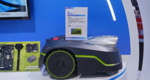
  Cologne, Germany – June 24, Fibocom, a global leader incommunication modules and AI solutions, had its state-of-the-art intelligentrobotic lawn mower solution prominently showcased at SPOGA+GAFA 2025, theworld’s leading trade fair for the garden and outdoor living industry. Multiplerobotic lawn mowers powered by Fibocom’s technology demonstrated seamlessnavigation across simulated garden environments—autonomously detectingboundaries, planning precise mowing routes, and avoiding obstacles—all withoutrelying on traditional physical perimeter wires. This impressive demonstrationhighlighted the disruptive potential of AI-driven, boundary-free lawn caresolutions.  The global smartrobotic mower market holds vast potential, with Europe and North Americaaccounting for 72% of the world’s 250 million private gardens. Yet, adoptionremains low—under 6% in North America and 10–30% in Europe—highlightingsubstantial room for growth as demand for intelligent lawn care accelerates.  Fibocom’ssolution integrates advanced AI vision, multi-sensor fusion, and intelligentnavigation to eliminate the need for traditional boundary wires. This enablesrobotic mowers to autonomously detect perimeters and obstacles, ensuring safe,efficient, and precise operation while significantly improving mowing productivity.It’s worth mentioning that, having accumulated over 350,000 kilometers ofreliable autonomous performance worldwide, this solution has proven itsrobustness in diverse and complex garden environments.  Fibocom provides two solution variantstailored to diverse customer needs: a standard pure-vision model and a flagshipversion combining binocular VIO (Visual-Inertial Odometry) with RTK (Real-TimeKinematic) for superior stability, precision, and large-area coverage—ideal forprofessional and commercial applications. This comprehensive suite, encompassingstereo cameras, AI processing boards, motor control units, and customizablemobile applications, enables OEM partners to accelerate product developmentcycles and focus resources on product differentiation and go-to-marketstrategies. For end users, it revolutionizes lawn care with smart mapping,autonomous operation, and auto-recharging for a safer, easier experience.  Strategic partnerships with top global brandsare fast-tracking the launch of Fibocom-powered products in key internationalmarkets over the next six months, underscoring Fibocom’s technologicalleadership and growing influence in the smart lawn care industry. Leveragingcutting-edge innovation and manufacturing excellence, Fibocom empowers partnersto penetrate top-tier European retail channels and scale globally, where everyimpeccably maintained lawn showcases the strength of Chinese smartmanufacturing on the world stage.
Key word:
Release time:2025-07-11 11:28 reading:1765 Continue reading>>
ROHM Releases New Level 3 SPICE Models Featuring Enhanced Simulation Speed
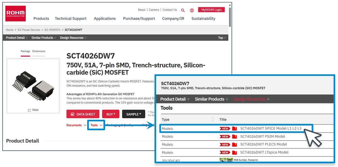
  ROHM has announced the release of new Level 3 (L3) SPICE models that deliver significantly improved convergence and faster simulation performance.  Since power semiconductor losses greatly impact overall system efficiency, simulation accuracy during the design phase is critical. ROHM’s earlier Level 1 SPICE models for SiC MOSFETs addressed this need by precisely replicating key device characteristics. However, challenges such as simulation convergence issues and prolonged computation times revealed the need for further refinement.  The new L3 models utilize a simplified approach that maintains both computational stability and accurate switching waveforms while reducing simulation time by approximately 50% compared to the L1 models. This allows for high-accuracy transient analysis of the entire circuits at significantly faster speed, streamlining device evaluation and loss assessment in the application design phase.  As of April 2025, ROHM has released 37 L3 models for its 4th Generation SiC MOSFETs, available for download directly from the Models & Tools section of each product page. The L1 models will continue to be offered alongside the new versions. A comprehensive white paper is also provided that facilitates model adoption.  The models can be downloaded from the Models & Tools section on individual 4th Generation SiC MOSFET product pages  Related Information  • White Papers  • Design Model Support Page  • SiC MOSFET Technical Documentation  Looking ahead, ROHM remains committed to advancing simulation technology to enable the design for higher-performance and more efficient applications, driving continued innovation in power conversion systems.
Key word:
Release time:2025-07-10 13:36 reading:1113 Continue reading>>
GigaDevice's GD5F1GM9 Series High-Speed QSPI NAND Flash Sets New Benchmark with Breakthrough Read Speeds for Accelerated Application Startup
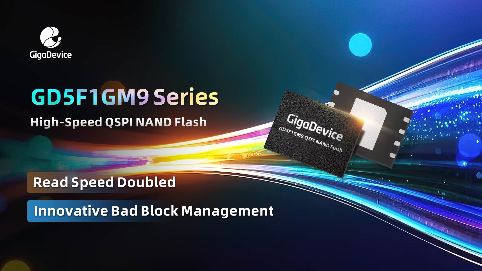
  GigaDevice, a leading semiconductor company specializing in Flash Memory, 32-bit Microcontrollers (MCUs), Sensors, Analog products and solutions, announces the launch of its GD5F1GM9 high-speed QSPI NAND Flash, which features breakthrough read speeds and innovative Bad Block Management (BBM) functionality.  The GD5F1GM9 series combines the high-speed read performance of NOR Flash with the large capacity and cost-effectiveness of NAND Flash. These innovations address key industry challenges of slow response times and vulnerability to bad block interference associated with traditional SPI NAND Flash. The GD51GM9 launch will open new growth opportunities for SPI NAND Flash, making it the ideal choice for fast-boot applications in sectors such as security, industrial, and IoT.  The GD5F1GM9 series high-speed QSPI NAND Flash is built on a 24nm process node. The series supports both 3V and 1.8V operating voltages as well as high-speed read modes including Continuous Read, Cache Read, and Auto Load Next Page. Continuous Read and Auto Load Next Page modes are newer read features added on this series, offering users versatile read options to further accelerate code and data fetch. These read modes utilize the new parallel computation approach for its ECC (Error Correction Code) design, replacing the previous serial computation method. This innovation significantly reduces the calculation time for the built-in ECC.  The 3V version of the series achieves a continuous read rate of up to 83MB/s in Continuous Read mode, operating at a maximum clock frequency of 166MHz. The 1.8V version has a continuous read rate of up to 66MB/s and supports a maximum clock frequency of 133MHz. The results in GD5F1GM9’s read speeds are up to 3 times faster than traditional SPI NAND products at the same frequency. These design advantages improve data access throughput, reduce system boot time, and lower overall system power consumption.  As bad blocks from the factory are inherent issues in NAND Flash, the GD5F1GM9 incorporates an on-chip Advanced Bad Block Management (BBM) to ensure comprehensive functionality of Continuous Read mode. Continuous Read allows read access of the full memory array with a single Read command in aid of the executed BBM that link bad block addresses to good block addresses. Read access will then automatically skip the bad block due to the established link access to the remap and linked good physical block address.  From the factory, the GD5F1GM9 series guarantees the first 256 blocks are good blocks. While there will be bad blocks from the factory and possible new bad blocks may arise during usage that needs to be managed, the BBM feature can create a logical block address to the physical block address link, allowing users to swap and replace bad blocks and the associated access will be on a good block once the BBM link is setup.  The device can support up to 20 Look Up Table BBM Links to further compliment Continuous Read mode functionality. This not only significantly improves resource utilization but also simplifies system design.  “Currently, the generally slow read speed of SPI NAND Flash has become a major bottleneck in enhancing boot performance of key applications,” said Ruwei Su, GigaDevice vice president and general manager of Flash BU, "The launch of GD5F1GM9 series high-speed QSPI NAND Flash sets a new performance benchmark in the market. This series effectively addresses the read speed limitations of traditional SPI NAND Flash and offers a new solution for bad block management, making it an ideal alternative for NOR Flash users with growing capacity needs. In the future, GigaDevice will continue to refine its underlying technologies to provide customers with more efficient and reliable storage solutions."  The GD5F1GM9 series offers 1Gb capacity with 3V/1.8V voltage options and supports WSON8 8x6mm, WSON8 6x5mm, and BGA24 (5×5 ball array) 5x5 ball package options. For detailed information and product pricing, please contact your local sales representative.  About GigaDevice  GigaDevice Semiconductor Inc. (SSE Stock Code 603986) is a global leading fabless supplier. The company was founded in April 2005 and headquartered in Beijing, China, with branch offices in many countries and regions worldwide, providing local support at customers' fingertips. Committed to building a complete ecosystem with four major product lines – Flash memory, MCU, sensor and analog – as the core driving force, GigaDevice can provide a wide range of solutions and services in the fields of industrial, automotive, computing, consumer electronics, IoT, mobile, networking and communications. GigaDevice has received the ISO26262:2018 automotive functional safety ASIL D certification, IEC 61508 functional safety product certification, as well as ISO9001, ISO14001, ISO45001, and Duns certifications. In a constant quest to expand our technology offering to customers, GigaDevice has also formed strategic alliances with leading foundries, assembly, and test plants to streamline supply chain management. For more details, please visit: www.gigadevice.com  *GigaDevice and their logos are trademarks, or registered trademarks of GigaDevice Semiconductor Inc. Other names and brands are the property of their respective owners.
Key word:
Release time:2025-04-23 17:09 reading:1936 Continue reading>>

Turn to

/ 10

  • Week of hot material
  • Material in short supply seckilling
model brand Quote
BD71847AMWV-E2 ROHM Semiconductor
CDZVT2R20B ROHM Semiconductor
MC33074DR2G onsemi
TL431ACLPR Texas Instruments
RB751G-40T2R ROHM Semiconductor
model brand To snap up
IPZ40N04S5L4R8ATMA1 Infineon Technologies
BU33JA2MNVX-CTL ROHM Semiconductor
TPS63050YFFR Texas Instruments
ESR03EZPJ151 ROHM Semiconductor
STM32F429IGT6 STMicroelectronics
BP3621 ROHM Semiconductor
Hot labels
ROHM
IC
Averlogic
Intel
Samsung
IoT
AI
Sensor
Chip

About us

Qr code of ameya360 official account

Identify TWO-DIMENSIONAL code, you can pay attention to

AMEYA360 mall (www.ameya360.com) was launched in 2011. Now there are more than 3,500 high-quality suppliers, including 6 million product model data, and more than 1 million component stocks for purchase. Products cover MCU+ memory + power chip +IGBT+MOS tube + op amp + RF Bluetooth + sensor + resistor capacitance inductor + connector and other fields. main business of platform covers spot sales of electronic components, BOM distribution and product supporting materials, providing one-stop purchasing and sales services for our customers.

Please enter the verification code in the image below:

verification code