NOVOSENSE's isolated driver with protection function helps enhance the safety and stability of the electronic control system in the new energy vehicle

发布时间:2024-02-29 14:26
作者:AMEYA360
来源:NOVOSENSE
阅读量:4817

  The main drive electronic control system is an important part of a new energy vehicle. This article will start from the system block diagram of the electronic control system, introduce the components of the system and their functions, and focus on the use of NOVOSENSE's single-channel isolated driver with protection function NSI6611, in the electronic control system: its Miller clamp function can well prevent short circuits; and the DESAT function can shut down IGBT / SiC in time when a short circuit occurs, protecting IGBT / SiC from damage and ensuring safe and stable operation of the system.

  Contents

  1)Introduction to the main drive electronic control system driver and the NSI6611-based driver board

  1. Composition of the main drive electronic control system

  2. Main chips on the driver board

  3. Interface definition

  4. NSI6611 application circuit

  2)Introduction to Miller clamp and the active Miller clamp function of NSI6611

  1. Miller effect

  2. Active Miller clamp

  3. Short circuit detection of power devices

  3)Introduction to the DESAT protection function of NSI6611

  1. DESAT detection peripheral circuit configuration and parameters

  2. DESAT protection timing

  3. Soft turn-off function

  1) Introduction to the main drive electronic control system driver and the NSI6611-based driver board

  1.1 Composition of the main drive electronic control system

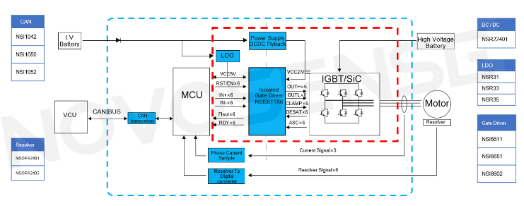
  The main drive electric control system consists of low voltage battery, VCU, MCU, high voltage battery and resolver three-phase motor. As shown in Figure 1 below, inside the blue dotted line is the main drive motor controller part and inside the red dotted line is the driver board that will be highlighted in this article.

  Functionally, the low voltage battery provides low voltage power supply for the system, and the VCU sends instructions to the electronic control system via the CAN bus and reads the status of the electronic control system; the high voltage battery provides high voltage power supply, and the Flyback circuit provides positive and negative voltages for the IGBT driver to drive the three-phase motor; the LDO (low dropout linear regulator) provides +5V power supply for the driver chip. NOVOSENSE's high voltage isolated driver NSI6611 is used to drive the IGBT and SiC modules; the current sampling circuit and resolver-to-digital converter are used to control motor operation.
NOVOSENSE's isolated driver with protection function helps enhance the safety and stability of the electronic control system in the new energy vehicle

  In the main drive electronic control system, NOVOSENSE provides a variety of chips, including the CAN interface chip, resolver-to-digital converter, power supply chip and high voltage isolated driver chip.

  1.2 Main chips on the driver board

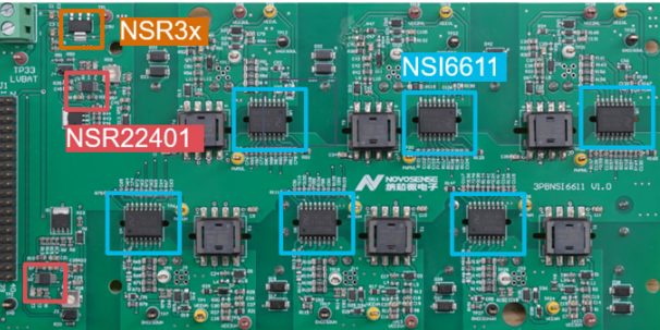
  Figure 2 below is a three-phase drive circuit board designed based on NOVOSENSE's single-channel smart isolated driver NSI6611. The six chips in the blue boxes are all NSI6611. The driver board also uses NOVOSENSE's Flyback power control chip NSR22401 to provide positive and negative voltages for the high voltage drive side of NSI6611; the LDO chip NSR3x provides 5V power supply for the low voltage side of NSI6611.
NOVOSENSE's isolated driver with protection function helps enhance the safety and stability of the electronic control system in the new energy vehicle

  NSI6611 is an automotive-grade, high voltage isolated gate driver with protection function that can drive IGBTs and SiCs, and it supports a peak voltage of up to 2121V and a maximum drive current of 10A without the need for an external drive circuit; CMTI (common-mode transient immunity) can be as high as 150kV/μs. In addition, it integrates active Miller clamp and DESAT (desaturation) protection, soft turn-off and ASC (active short circuit) functions internally, with an operating temperature range of -40°C to +125°C.

  1.3 Interface definition

  As shown in Figure 3 below, the left side of the driver board is the signal interface between the driver board and the control board, including 6 input signals provided by the control board for PWM control; 6 FAULT output signals provided to the control board when NSI6611 detects IGBT overcurrent or undervoltage; 6 Ready output signals used to indicate whether the NSI6611 power supply is undervoltage; and 2 RESET input signals that control 3 high sides and 3 low sides respectively. The right side of the driver board is the power interface, and the power supply voltage range is 9V to 16V.

  1.4 NSI6611 Application Circuit

  Figure 4 below is the drive circuit of NSI6611. The left side is the low voltage control side. The 100Ω resistor connected in series on the signal line can effectively reduce signal reflection; since the Fault and Ready signals have an internal Open Drain structure, a 5.1kΩ pull-up resistor needs to be added. In addition, the RC circuit composed of the PWM signal and a 1nF capacitor can filter out high-frequency signals, and a 0.1μF decoupling capacitor is added to VCC1.

  The right side is the high voltage drive side. Two 1206 package gate resistors are connected in parallel. The gate has a 10k pull-down resistor. The gate capacitance can be adjusted for different applications. The CLAMP pin is connected to the GATE through a 0Ω resistor.

  2) Introduction to Miller clamp and the active Miller clamp function of NSI6611

  2.1 Miller effect

  The Miller effect refers to the phenomenon in a transistor or field effect tube that the capacitance at the output of the amplifier increases due to the interaction between the input capacitance and the gain of the amplifier. It can not only increase switching delay, but also cause parasitic turn-on.

  Due to the inherent characteristics of semiconductors, there are various parasitic capacitances inside the IGBT. The capacitance between the gate and collector is called Miller capacitance. It is often seen in tests that the gate voltage does not rise directly to the VCC voltage, but rises to a voltage plateau, maintains for a period of time and then rises again. This voltage plateau is the Miller plateau, which is generated by Miller capacitance.

  Miller capacitance may also cause false turn-on of the low side. Typically, motor drives require the use of the high and low sides. When Q2 is turned off and Q1 is turned on, a certain current will be generated due to the high dv/dt and Miller capacitance. We can calculate the current by using the formula I=C * dv/dt. The current flowing through the gate resistor will generate a VGE voltage. When this voltage exceeds the turn-on threshold of Q2, Q2 will turn on, and at this time, Q1 is already in the ON state, thus causing a shoot-through short circuit.

  2.2 Active Miller clamp

  In order to solve the problem of shoot-through caused by the Miller effect, negative voltage turn-off can be used, but this will increase the complexity of the power supply design and increase the BOM cost; the second option is to use a driver chip with Miller clamp function to control the IGBT turn-off process.

  The IGBT turn-off process controlled by a driver chip with Miller clamp function is shown in Figure 6 below. First, the OUTL pin is turned on, causing the gate voltage to drop; when the gate voltage drops below the CLAMP threshold, the CALMP pin is turned on, causing the OULT pin to turn off. The resulting path can effectively bypass the gate resistor, thus avoiding the phenomenon of shoot-through. It is worth noting that the Miller clamp module only works when the IGBT is turned off.

  2.3 Short circuit detection of power devices

  IGBT and SiC devices vary in their short circuit capabilities. Before using a power device to design a drive system, you must first understand its basic parameters such as maximum voltage, maximum current and Rdson (on-resistance). Short-circuit capability is also a parameter worthy of focus, since the short circuit characteristics of the device need to be known when short circuit protection is designed.

  Take the short circuit characteristic parameters of the IGBT as an example. At 25°C, its maximum short circuit time is 6μs, which means that the IGBT needs to be turned off in time within 6μs. When the short circuit current reaches 4800A, the value is already several times the normal operating current. Once a short circuit occurs, a large amount of heat will be generated instantly, causing the junction temperature to rise sharply. If it is not turned off in time, the device will be burned and there is even a risk of fire. This must be avoided in system design.

  Generally, the short circuit time of IGBT can reach up to 10μs, while the short circuit time of SiC is only 2~3μs, which brings great challenges to short circuit protection. Therefore, short circuit must be detected and turn-off must be performed in time.

  Method 1 is current detection. A resistor is connected in series with the IGBT, or a current sensor is used to directly detect the overcurrent condition. However, this will increase the cost significantly and make the circuit system more complex.

  Method 2 is desaturation detection, also known as DESAT protection. As shown in Figure 7 below, we can see from the graph of VCE voltage and collector current that when VCE is less than 0.4V, no current flows through the cut-off region; as the VCE voltage increases, the current also increases and a saturation region appears, and then it enters the linear region, i.e., the desaturation region.

  Usually, when the IGBT works in the saturation region, it will enter the desaturation region once a short circuit occurs. It can be seen that the VCE voltage generally does not exceed 2V in the saturation region; if it enters the desaturation region, VCE will rise rapidly and even reach the system voltage. Desaturation detection is to detect whether the IGBT has entered the desaturation region by detecting the VCE voltage.

  3) Introduction to the DESAT protection function of NSI6611

  3.1 DESAT detection peripheral circuit configuration and parameters

  DESAT detection consists of NSI6611 and external DESAT capacitor, resistor and high voltage diode. The NSI6611 chip integrates a 500μA constant current source and comparator internally.

  When the IGBT is turned on normally, the VCE voltage is very low, basically below 2V, and the diode is in a forward turn-on state. The voltage value of VDESAT is equal to the voltage drop of the resistor plus the voltage drop of the diode, plus the VCE voltage. Assuming that the resistance of the resistor is 100Ω, the forward voltage drop of the diode is 1.3V, and VCE is 2V, then, according to the formula in Figure 8, we can get: When the IGBT is turned on normally, the voltage detected by DESAT is basically less than 3.35V.

  When the IGBT is short-circuited, the VCE voltage will rise rapidly. At this time, the diode is in the OFF state, and the current will flow to the DESAT capacitor and charge it. Since the DESAT current of NSI6611 is 500μA and the DESAT threshold is 9V, this means that a capacitor needs to be matched to charge the DESAT capacitor to 9V at 500μA within the short circuit time.

  Assuming that the DESAT capacitance is 56pF, according to the capacitor charging formula in Figure 8: the charging time of the capacitor is about 1μs; plus the blanking time of 200ns and the filtering time of 200ns, the total short circuit protection response time is 1.4μs. This time is not only shorter than the safe short circuit time of IGBT, but also shorter than the safe short circuit time of SiC.

  3.2 DESAT protection timing

  Figure 9 below is the DESAT protection timing diagram. It can be seen from the figure that in step 1, GATE rises and DESAT starts the blanking time; in step 2, the blanking time ends and the DESAT current is turned on, and if the IGBT is short-circuited, the diode enters the cut-off state and the DESAT current charges the capacitor; in step 3, when the DESAT capacitor is charged to the threshold of 9V, the filtering time of DESAT protection starts; in step 4, the filtering time ends and GATE is turned off.

  Figure 9: DESAT protection timing diagram

  3.3 Soft turn-off function

  As mentioned above, GATE is turned off when a DESAT fault is detected. So, is it enough to just turn it off normally? Not really. When a short circuit occurs, the IGBT current is at least 6 to 8 times the normal current. According to the formula, the voltage is equal to the stray inductance of the system multiplied by di/dt (V=Ls*di/dt). If such a large current is turned off quickly, a large VCE voltage will inevitably be generated, which is enough to damage the IGBT. There are only two ways to reduce VCE overshoot: one is to reduce stray inductance, and the other is to reduce di/dt.

  Firstly, due to the parasitic parameters of the device, PCB routing, structural design, etc., there is inevitably a certain amount of stray inductance; secondly, to reduce di/dt, under the premise of a certain current, the only way is to increase the turn-off time, that is, let the IGBT turn off slowly for safe turn-off. NSI6611 can provide 400mA soft turn-off, thereby suppressing VCE overshoot and effectively solving the problem of device protection.

(备注:文章来源于网络,信息仅供参考,不代表本网站观点,如有侵权请联系删除!)

在线留言询价

相关阅读
High Cost-Effectiveness for RS485 Isolation: NOVOSENSE Launches the SP301H/L Series Three-Channel Digital Isolators
  NOVOSENSE announced the launch of the SP301H/L series, a family of three-channel digital isolators built on its proprietary third-generation capacitive isolation technology. Designed specifically for RS485 communication isolation applications, the SP301H/L series delivers comprehensive improvements in data rate, power consumption, electromagnetic immunity, and package size.  Compared with the previous-generation SP301A and NIRS31 series products, the SP301H/L supports communication speeds of up to 8 Mbps, features a low quiescent current design, and offers enhanced electromagnetic immunity performance. Housed in a compact SSOW10 wide-body package with fine-pitch leads, the device achieves higher integration while significantly reducing PCB size, providing customers with a high-performance, highly reliable, and cost-effective isolation solution.  RS485 communication is widely used in power metering terminals, industrial automation systems, and renewable energy storage applications due to its long transmission distance, strong noise immunity, and flexible multi-node networking capability. In these applications, isolation devices play a critical role in ensuring communication reliability and system safety. Conventional RS485 isolation solutions based on three optocouplers suffer from limitations such as high component count, restricted bandwidth, aging-related performance drift, and large PCB footprint, making them increasingly unable to meet the demands of high-speed communication, long service life, and compact system design. As system performance requirements continue to increase, digital isolation is becoming the preferred approach for next-generation RS485 isolation solutions.  High Cost-Effectiveness: Replacing Three Optocouplers with a Single Chip for Simplified Design and Lower System Cost  Traditional isolated RS485 communication solutions typically require three optocouplers together with multiple external resistors and capacitors, resulting in a complex BOM list, higher procurement and inventory management costs, and increased PCB space consumption. By integrating three isolation channels into a single device, the SP301H/L directly replaces discrete optocouplers and their supporting circuitry, significantly simplifying the BOM, reducing component count and routing complexity, and improving overall system integration.  The SP301H/L adopts a compact SSOW10 wide-body package, reducing PCB size by more than 60% compared to conventional optocoupler-based solutions and freeing up valuable board space for system designers.  In terms of performance, the SP301H/L supports data rates up to 8 Mbps on the data channel and up to 1 Mbps on the enable control channel, effectively overcoming the bandwidth limitations of traditional optocouplers. This enables high-speed, low-latency communication required by applications such as smart electricity meters and industrial fieldbus networks. To support different system architectures, the SP301H features a default-high enable pin, while the SP301L features a default-low enable pin, providing greater flexibility for MCU enable-logic implementation.  The device also features a low quiescent current design, making it suitable for battery-powered equipment and field instruments with stringent power consumption requirements. With an operating ambient temperature range of –40°C to +125°C, the SP301H/L fully meets industrial-grade application requirements. Combining high integration, compact packaging, strong performance, and simplified external circuitry, the SP301H/L enables seamless migration from optocoupler-based solutions while addressing the growing demand for miniaturization, lightweight design, and high reliability in smart metering and industrial systems.  High Reliability: Comprehensive Immunity Enhancement for Stable Communication Operation  Smart electricity meters are typically deployed in complex electromagnetic environments where communication links must withstand power-grid surges, switching noise, and interference introduced by long-distance cabling. Through optimized isolation architecture and enhanced immunity design, the SP301H/L significantly improves electromagnetic susceptibility (EMS) performance for RS485 communication links, reducing bit-error rates and communication interruptions while ensuring stable and reliable data transmission.  Compared with the previous-generation SP301A and NIRS31 series, the SP301H/L delivers substantial improvements in electromagnetic robustness:  ·EOS (Electrical Overstress) tolerance is improved by approximately 10%, with latch-up immunity exceeding 10 V. This significantly enhances resistance to power-supply overstress conditions, reducing the risk of damage caused by abnormal power fluctuations and extending overall system lifetime.  ·Excellent power-supply noise immunity enables the device to maintain normal operation and error-free communication even under high-frequency, high-amplitude system noise interference in the MHz range, improving reliability in harsh electromagnetic environments.  ·Common-mode transient immunity (CMTI) reaches a typical value of 200 kV/μs, effectively suppressing common-mode transient disturbances and ensuring accurate and stable signal transmission.  In addition, the SP301H/L is built on NOVOSENSE’s industry-leading third-generation capacitive isolation technology, delivering outstanding isolation performance. The device supports an isolation withstand voltage of up to 5 kVrms (1 minute) and surge voltage capability exceeding 10 kV, meeting reinforced insulation requirements.  Comprehensive “Isolation+” Portfolio Setting New Benchmarks for Isolation ICs  Leveraging its extensive expertise and technological leadership in isolation technologies, NOVOSENSE offers a comprehensive “Isolation+” product portfolio covering digital isolators, isolated sensing solutions, isolated interfaces, isolated power supplies, and isolated gate drivers. Together, these products form a complete ecosystem designed to provide robust safety barriers for high-voltage systems.  ·“+” Represents Enhanced Safety: NOVOSENSE Isolation+ products deliver safety performance beyond basic isolation standards, helping customers establish stronger safety boundaries between high- and low-voltage domains.  ·“+” Represents a Complete Product Ecosystem: Built upon NOVOSENSE’s mature capacitive isolation IP platform, the Isolation+ portfolio encompasses digital isolators, isolated sensing devices, isolated interfaces, isolated power supplies, and isolated drivers, providing customers with a comprehensive one-stop isolation solution.  ·“+” Represents Deep Application Enablement: NOVOSENSE Isolation+ products address the critical requirements of high-voltage electric vehicle platforms, high-power solar, energy storage and EV charging systems, and highly integrated, high-efficiency AI server power supplies, enabling system-level safety, reliability, and efficiency.  As of 2025, cumulative shipments of NOVOSENSE isolation-related ICs have exceeded 2.7 billion units. As a global leading supplier of isolation ICs, NOVOSENSE remains committed to advancing isolation technology through its comprehensive Isolation+ portfolio, leveraging core isolation IP and a complete product ecosystem to deliver one-stop isolation solutions for customers worldwide.
2026-07-22 13:25 阅读量:705
Visit NOVOSENSE at PCIM Europe 2026!
  We warmly invite you to visit NOVOSENSE at PCIM Europe 2026. Discover how NOVOSENSE empowers innovation across automotive electronics, renewable energy & power supply, and industrial control with a comprehensive portfolio of isolators, interfaces, drivers, sensors, signal chain, and power management ICs.  Date: June 9–11, 2026  Venue: Nuremberg Exhibition Centre, Germany  Booth: Hall 4A, Booth 119  ✦ What to Expect ✦  Functional safety ICs for safety-critical automotive systems  One-stop body control & automotive lighting solutions  SerDes and ultrasonic radar IC solutions for smarter mobility  Technical presentations on high-voltage electric mobility and AI data center power systems  ✦ Highlights Preview ✦  Functional Safety ICs for Safety-Critical Automotive Systems  Isolated gate driver NSI6911F — certified by TÜV Rheinland to meet ISO 26262 ASIL D requirements, featuring up to 19A peak drive capability, ±150kV/μs CMTI, an integrated 12-bit isolated ADC, and advanced diagnostic functions for high-voltage applications such as traction inverters, OBCs, and DC-DC converters.  ASIL B ultrasonic radar ASSP NSUC1800 and LED driver NSL21924FS , reflecting NOVOSENSE's expanding functional safety portfolio across sensors, signal chain, power management, and driver ICs.  One-Stop Automotive Body Control & Lighting Solutions  For BCM and ZCU applications, NOVOSENSE offers motor driver products for brushed DC motors, stepper motors, BLDC motors, relays, valves, and solenoids, supporting efficient, precise, and safe motor control.  For automotive lighting, NOVOSENSE will showcase full-scenario LED driver solutions for ambient lighting, reading lights, headlighting, rear lighting, ISD/ISC lighting, grille lighting, and more, helping create safer, smarter, and more distinctive vehicle lighting experiences.  Enabling Smarter Mobility with SerDes and Ultrasonic Radar IC Solutions  SerDes chipset — NLS9116 single-channel serializer and NLS9246 four-channel deserializer, designed for cameras, displays, and domain controllers in ADAS and intelligent cockpit systems.  AK2 ultrasonic radar ASSP — comprising the NSUC1800 sensor-side chip and NSUC1802 host-side interface conversion chip, providing a turnkey solution for applications such as UPA and APA.  ✦ Keynote Speeches ✦  Join NOVOSENSE experts at PCIM Europe 2026 for in-depth technical presentations on how advanced semiconductor technologies are addressing the evolving demands of high-voltage electric mobility and AI data center power systems.  E-Mobility & Energy Storage Stage  Hall 6, Booth 220  Topic: Evolution and Challenges of Gate Driver Technology for New Generation of xEV Powertrain System  Time: June 9, 2026 | 15:25–15:45 (GMT+1)  Speaker: Timmy Wu  Topic: Enabling EV High-Voltage Safety with Advanced Isolated Sensing  Time: June 11, 2026 | 12:05–12:25 (GMT+1)  Speaker: Lillian Liu  AI & Data Centers Stage  Hall 5, Booth 320  Topic: Power Density Scaling in AI Data Centers: From System Constraints to Semiconductor Device Challenges  Time: June 9, 2026 | 14:35–14:55 (GMT+1)  Speaker: Wenzhe Xu
2026-05-14 11:40 阅读量:1676
NOVOSENSE Launches Next-Generation Isolated CAN Transceiver NSI1150, Supporting ±70V Bus Fault Protection and Higher Data Rates
  NOVOSENSE today announced the launch of its new industrial-grade isolated CAN transceiver, the NSI1150 series. Built on NOVOSENSE's third-generation isolation technology, the device delivers ±70V bus fault protection and up to ±150kV/μs (typical) common-mode transient immunity (CMTI). Compared to the previous generation (NSI1050), the NSI1150 achieves a comprehensive improvement in reliability and noise immunity. It also integrates NOVOSENSE's proprietary CAN FD transceiver, supporting communication speeds of up to 5 Mbps.  The NSI1150 is available in multiple package options, including SOW16, SOW8, SOP8, SOWW8, and DUB8, addressing diverse design requirements. It is well suited for high-voltage, high-noise, multi-node applications such as industrial automation and control, energy and power systems, as well as communications and servers.  Reliability Upgrade for Harsh Environments  The NSI1150 delivers industry-leading reliability and robustness, featuring a high CMTI of ±150kV/μs (typical) and ±70V bus fault protection, enabling it to effectively handle strong electromagnetic interference and ground potential differences in demanding environments.  In addition, all pins support ±6kV HBM ESD protection and 10kV surge capability across the isolation barrier, ensuring stable communication even under extreme conditions. The device offers multiple isolation ratings—3 kVRMS, 5 kVRMS, and 7.5 kVRMS—to meet stringent safety requirements across various applications, reinforcing system protection in critical sectors such as industrial automation and energy infrastructure.  Multiple Package Options for Flexible Design  The NSI1150 is offered in five mainstream package options—SOW16, SOW8, SOP8, SOWW8, and DUB8—accommodating different space constraints and safety requirements. Among them, the newly introduced SOWW8 wide-body package provides up to 15 mm creepage distance, making it ideal for applications with strict creepage requirements, such as photovoltaic systems, EV charging stations, and industrial power supplies.  This extended creepage distance simplifies safety certification processes and enables more flexible layout design for high power density systems. The diversified package portfolio further enhances design flexibility and accelerates time-to-market.  "Isolation+" Portfolio Setting Industry Benchmark  Leveraging its deep expertise and technological leadership in isolation, NOVOSENSE offers a comprehensive "Isolation+" portfolio, including digital isolators, isolated sensing, isolated interfaces, isolated power, and isolated drivers.  NOVOSENSE is building a robust safety foundation for high-voltage systems with its full "Isolation+" ecosystem:  "+" stands for enhanced safety: NOVOSENSE products deliver safety levels exceeding basic isolation standards, and build a more reliable system isolation safety boundary for customers' systems.  "+" stands for full product ecosystem: With mature capacitive isolation technology IP as the cornerstone, expand into a complete product portfolio to provide one-stop isolation solutions.  "+" stands for in-depth application empowerment: Meet the emerging needs of scenarios including electric vehicle high-voltage platforms, high-power photovoltaic-storage-charging systems, and high-integration, high-efficiency AI server power supplies, enabling system-level safety, reliability and efficiency.  With its comprehensive "Isolation+" product strategy—anchored by core technology IP and a full ecosystem—NOVOSENSE continues to set the benchmark in isolation semiconductors, delivering one-stop isolation solutions to customers worldwide.  Previous:
2026-04-24 10:58 阅读量:1650
NOVOSENSE and Inovance Automotive Co-Develop IC Solutions for Next-Generation Electric Drive Platforms
  NOVOSENSE Microelectronics announced that two highly integrated ICs—an isolated sensing IC and a logic ASC IC—developed in close collaboration with Inovance Automotive, a leading supplier of intelligent electric vehicle components and solutions, have entered mass production on Inovance Automotive’s next-generation electric drive (e-drive) platform. The customized IC solutions offer higher integration and optimized performance, supporting the ongoing shift toward more integrated electric drive systems while enabling designs that meet increasingly stringent functional safety requirements.  Conventional discrete electric drive designs rely on widely distributed components and complex wiring, often resulting in larger system size, higher power losses, slower response, and constrained reliability. As electric vehicles continue to demand longer driving range and higher output power, electric drive architectures are moving rapidly toward multi-in-one and highly integrated designs. In this context, semiconductor solutions must deliver greater functional integration while maintaining accuracy, reliability, and functional safety margins within limited space, without constraining system-level design flexibility.  Building on more than a decade of experience in motor controller system architectures and functional safety, Inovance Automotive proactively defined the key functional and performance requirements for the isolated sensing IC and logic ASC IC at an early stage of development. In response to these requirements, NOVOSENSE integrated high-voltage LDO, isolated sensing amplifier, and isolated comparator into a single isolated sensing IC. This integration significantly reduces external component while enabling high-precision isolated voltage sensing, fast OV/UV protection, and more compact electric drive designs.  The customized logic ASC IC further integrates multiple logic functions and supports frequency detection, enabling centralized handling of interface-related logic. This approach simplifies interface design, improves overall system integration, and supports more compact inverter layouts. At the same time, it helps reduce BOM cost and provides a solid foundation for optimizing functional safety architectures in electric drive and traction inverter systems.  By replacing mature discrete circuits with integrated IC solutions, the collaboration delivers clear system-level benefits.  Simplified architectures and fewer components reduce potential failure points and improve overall product robustness.  Higher integration lowers PCB area requirements, creating additional headroom for increased power density.  Standardized IC solutions also streamline development by reducing design and validation effort, helping shorten development cycles and accelerate time-to-market.  "Electric drive systems are entering a phase where higher integration is becoming essential, and progress at the chip level increasingly translates into system-level advantages," said Zheng Chao, Director of the R&D Center at Inovance Automotive. "This collaboration combines our strengths in electric drive systems with NOVOSENSE’s expertise in automotive semiconductors. More importantly, it reflects an important capability upgrade for Inovance Automotive—we are not only developing high-performance power electronics products, but also participating from the outset in defining system architectures and core chips. We look forward to continuing our work with NOVOSENSE to shape next-generation electric drive platforms and deliver more competitive system solutions to OEMs."  "NOVOSENSE and Inovance Automotive have established a strong foundation for collaboration," said Ye Jian, Product Line Director at NOVOSENSE. "This project demonstrates both our customer's confidence in our technology and our application-driven approach to innovation. By drawing on our long-standing expertise in isolation and interface technologies, we will continue to deliver high-precision, high-performance, and high-reliability IC solutions to support Inovance Automotive's next-generation electric drive platforms."  NOVOSENSE's Isolation+ portfolio covers digital isolator, isolated sensing, isolated driver, isolated power, and isolated interface, with cumulative shipments exceeding two billion units as of October 2025. The company also offers a broad automotive interface portfolio—including CAN, LIN, SerDes, logic ICs, and level shifters—providing customers with one-stop automotive-grade isolation and interface solutions. Across the new energy vehicle electrical system, NOVOSENSE works with hundreds of component suppliers, delivering semiconductor solutions for traction inverter, onboard charger (OBC), DC/DC converter, and battery management system (BMS), spanning sensor, signal chain, power management IC, and MCU.
2026-02-25 17:36 阅读量:2067
  • 一周热料
  • 紧缺物料秒杀
型号 品牌 询价
RB751G-40T2R ROHM Semiconductor
CDZVT2R20B ROHM Semiconductor
BD71847AMWV-E2 ROHM Semiconductor
TL431ACLPR Texas Instruments
MC33074DR2G onsemi
型号 品牌 抢购
STM32F429IGT6 STMicroelectronics
ESR03EZPJ151 ROHM Semiconductor
BU33JA2MNVX-CTL ROHM Semiconductor
IPZ40N04S5L4R8ATMA1 Infineon Technologies
TPS63050YFFR Texas Instruments
BP3621 ROHM Semiconductor
热门标签
ROHM
Aavid
Averlogic
开发板
SUSUMU
NXP
PCB
传感器
半导体
相关百科
关于我们
AMEYA360微信服务号 AMEYA360微信服务号
AMEYA360商城(www.ameya360.com)上线于2011年,现 有超过3500家优质供应商,收录600万种产品型号数据,100 多万种元器件库存可供选购,产品覆盖MCU+存储器+电源芯 片+IGBT+MOS管+运放+射频蓝牙+传感器+电阻电容电感+ 连接器等多个领域,平台主营业务涵盖电子元器件现货销售、 BOM配单及提供产品配套资料等,为广大客户提供一站式购 销服务。

请输入下方图片中的验证码:

验证码