TSMC’s Roadmap Full, But Thin

发布时间:2018-05-03 00:00
作者:Ameya360
来源:Rick Merritt
阅读量:1792

Continuing to move fast in multiple directions at once, TSMC announced that it is in volume production with a 7-nm process and will have a version using extreme ultraviolet (EUV) lithography ramping early next year. In addition, it gave its first timeline for a 5-nm node and announced a half-dozen new packaging options.

Meanwhile, the foundry is pushing power consumption and leakage down on more mainstream 22-/12-nm nodes, advancing a laundry list of specialty processes and rolling out an alphabet soup of embedded memories. At the same time, it is exploring future transistor structures and materials.

Overall, the Taiwanese giant expects to make 12 million wafers this year with R&D and capex spending both on the rise. It has even started production of 16-nm FinFET chips in Nanjing, a big first for China.

The only bad news is that the advantages with the new process nodes are getting thinner. The new normal for performance gains and power reductions generally fall in a 10% to 20% range, a reality that makes the new packaging and specialty processes increasingly important.

TSMC is in volume production of 7-nm chips today with more than 50 tapeouts expected this year. It’s making CPUs, GPUs, AI accelerators, cryptocurrency mining ASICs, networking, gaming, 5G, and automotive chips.

The node delivers 35% more speed or uses 65% less power and sports a 3x gain in routed gate density. By contrast, the N7+ node with EUV will only deliver 20% more density, 10% less power, and apparently no speed gains — and those advances require use of new standard cells.

TSMC has validated in silicon what it calls foundation IP for N7+. However, several key blocks will not be ready until late this year or early next year, including 28–112G serdes, embedded FPGAs, HBM2, and DDR5 interfaces.

Expect 10% to 20% more effort laying out IP for the EUV process, said Cliff Hou, vice president of R&D for design and technology platforms. “We developed a utility to migrate IP with incremental effort.”

Fully certified EDA flows for N7+ will be ready by August. Meanwhile, yields of a test 256-Mbit SRAM at N7+ are as good as yields were for the early 7-nm node, he said.

Looking ahead, TSMC aims to start risk production of a 5-nm node in the first half of 2019, focusing on mobile and high-performance computing chips.

Compared to the initial 7 nm without EUV, the 5-nm node promises a 1.8x greater density than 7 nm. However, it is only expected to reduce power by up to 20% or raise speeds by about 15%, perhaps 25% using Extremely Low Threshold Voltage (ELTV), details of which TSMC has not yet provided.

“Without EUV, they can’t deliver the same scaling advantage as past nodes,” said Mike Demler, an analyst with the Linley Group. “If you look at N7+, they claim an additional 20% scaling over N7. So EUV is required to get closer to traditional Moore’s Law scaling. Their N5–N7 scaling just gets worse.”

TSMC clearly has a bead on high-volume manufacturing for EUV early next year. It got systems to sustain production at 250 W for a couple of weeks in April and aims to hit 300 W next year, a power level needed for volume throughput.

With average daily power levels at 145 W, the foundry has a ways to go, but “throughput is on track to meet production needs,” said Y.J. Mii, vice president of R&D for technology development.

Besides “significant progress on power and throughput,” Mii reported that resist dosage is declining toward the foundry’s 1Q19 production goal, though it’s still about a third too high. The protective pellicle transmits 83% of EUV light and should hit 90% next year.

EUV continues to provide much better uniformity of critical dimensions than immersion steppers, said Mii, showing several examples. The foundry expects to use EUV on multiple layers in both N7+ and 5-nm nodes and is aggressively installing NXE3400 systems from ASML.

It appears that TSMC’s EUV plan is within six months of the production schedule of Samsung, which has said that it will be in production this year. The South Korean giant plans its own event later this month, where it will provide an update on its progress.

The gap is not likely enough to get large-volume customers such as Apple or Qualcomm to switch suppliers. In the long term, a lead of a few months will be insignificant, said G. Dan Hutcheson, chief executive of market watcher VLSI Research.

Meanwhile, TSMC’s 5-nm node is still embryonic with a version 0.5 EDA flow targeted for June release and a v0.5 design kit in July. Many IP blocks won’t be validated until next year, including PCIe Gen 4, DDR4, and USB 3.1 interfaces.

By the end of 2019, the foundry aims to triple to 1.1 million wafers/year its production on 10-/7-nm nodes. It’s latest fab complex 18 is under construction in Taiwan now and aims to start 5-nm production in 2020.

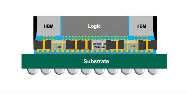
Now that TSMC has established its 2.5-D CoWoS package in GPUs and other processors and its wafer-level fan-out InFO in smartphone chips, it is expanding both offerings and adding others.

CoWoS chips will have options for silicon interposers up to twice a reticle’s size, apparently stitched in the field, starting early next year. Versions with 130-micron bump pitch will be qualified this year.

The InFO technique is getting four cousins. Info-MS, for memory substrate, packs an SoC and HBM on a 1x reticle substrate with a 2 x 2-micron redistribution layer and will be qualified in September.

InFO-oS has a backside RDL pitch better matched to DRAM and is ready now. A multi-stacking option called MUST puts one or two chips on top of another larger one linked through an interposer at the base of the stack.

Finally, InFO-AIP stands for antenna-in-package, sporting a 10% smaller form factor and 40% higher gain. It targets designs such as front-end modules for 5G basebands.

“InFO is an important platform,” said Jan Vardaman, a veteran packaging analyst and president of TechSearch International.

“TSMC’s InFO for baseband/modem package in a PoP with memory is very impressive — lower profile, smaller form factor, and better performance. InFO on Substrate is going to be popular because it’s 2-micron lines and spaces will cover a lot of applications.”

But that’s not all. TSMC introduced two wholly new packaging options.

A wafer-on-wafer pack (WoW) directly bonds up to three dice. It was released last week, but users need to ensure that their EDA flows support the bonding technique. It will get EMI support in June.

Finally, the foundry roughly described something that it called system-on-integrated-chips (SoICs) using less than 10-micron interconnects to link two dice, but details are still sketchy for the technique to be released sometime next year. It targets apps from mobile to high-performance computing and can connect dice made in different nodes, suggesting it may be a form of system-in-package.

“It used to be ASE leading the way in packaging, but now I’d say TSMC is,” said one analyst during a break.

The motivations are clear. As the advantages of CMOS scaling diminish, packaging helps deliver performance, in part through faster memory access. In the last few years, TSMC, which runs three back-end production lines, won significant business with Apple in part due to InFO and Xilinx and Nvidia in part with CoWoS.

The new packages “look like the long-promised alternative to the end of Moore’s Law, but pretty expensive and still with lots of issues,” said Demler of Linley Group.

Only about a third of TSMC’s business is at advanced nodes such as 28 nm and beyond. Thus, the foundry discussed advances in a laundry list of specialty processes as well as advances a step or two back from the bleeding edge.

For example, it is developing ultra-low-power and ultra-low-leakage versions of its 22-nm planar and 12-nm FinFET nodes. They will compete with FD-SOI processes ramping at Globalfoundries and Samsung.

The new 22-nm versions use 28-nm design rules and deliver a 10% optical shrink and speed gain or can reduce power 20%. The process and related IP will be ready by the end of the year with target apps including advanced microcontrollers, IoT, and 5G millimeter-wave chips.

The 12-nm versions use FinFETs and more compact cell libraries to deliver about 16% more speed than TSMC’s 16FFC. High-speed serdes are among the few pieces of IP that won’t be ready until next year.

In memories, a 40-nm resistive RAM is now ready as an alternative to flash for IoT chips. It adds just two mask layers and sports 10 years of retention and support for 10,000 cycles.

A 22-nm embedded MRAM will debut this year that’s faster and has longer retention than flash. It targets automotive, mobile, and high-performance designs with good yields on test chips so far.

Separately, TSMC is delivering smaller form factors for MEMS. It expects GaN-on-silicon with 10-V and 650-V driver integration in the fall and 100-V D-HEMT qualified next year for cellular power amps.

In addition, the foundry has qualified EDA flows and IP for its 16FFC process for automotive. It plans to have a 7-nm automotive process ready by the end of the year, though full certification will take until 2Q19.

As icing on the cake, TSMC announced a milestone in China, sketched out its long-term research, and gave an update on its use of machine learning for process automation.

The foundry is now producing 16-nm FinFET chips in its new Nanjing fab several months earlier than planned. The first phase in place includes a spaceship-like cafeteria, tubular office building, and 20,000-wafers/month fab that rivals Apple’s new headquarters in flashy design, though not scale. A second phase eventually will double production.

Meanwhile, TSMC researchers are progressing on designs of stacked nanowires as nanosheets for a next-generation transistor suitable for work at 2 nm and beyond. The design sports better electrostatics than FinFETs and can be optimized for power and performance by adjusting device width.

The foundry sees germanium as a strong candidate to replace silicon, providing lower power at the same speed. It achieved a record-low contact resistance using the material in a CMOS-compatible dielectric.

TSMC is exploring a variety of 2D back-end materials including molybdenum disulfide for their atomically smooth surfaces. They also are examining novel ways to enlarge copper grains to reduce resistance in interconnects. In addition, they are working on a selective dielectric-on-dielectric deposition process to enable self-aligning of copper vias.

In memories, they are exploring embedded MRAM for use beyond the 22-nm node, possibly with alternative magnetic structures. For embedded ReRAM beyond 40 nm, high-density crossbars are seen as an energy-efficient approach, especially for AI accelerators.

In terms of automation, TSMC is embracing machine learning to systematically analyze its wealth of wafer-processing data. It already tunes process recipes for specific tools and products. It also tracks and classifies process variations in an effort to automate the discovery of whether a problem is in a tool, process, or material.

The company has a library of more than 50,000 process recipes and tens of millions of control charts. Just how TSMC is applying machine learning to its automation tasks and with what products was unclear — no doubt, still something of a work in progress, perhaps with some secret sauce.

(备注:文章来源于网络,信息仅供参考,不代表本网站观点,如有侵权请联系删除!)

在线留言询价

相关阅读
TSMC Plans Mini-Loop at Kaohsiung to Speed CoWoS Tool Validation; Reportedly Eyes AUO Site for CoPoS
  As AI demand drives growth in advanced packaging, TSMC is strengthening equipment and materials validation across its supply chain. According to Commercial Times, construction of Kaohsiung’s Baipu Industrial Park began on September 21, with TSMC expected to anchor the cluster. The company plans to set up a modular “Mini-Loop” line to validate new equipment and process integration before the equipment is introduced into CoWoS (Chip-on-Wafer-on-Substrate) production, aiming to improve validation efficiency by 25% to 50%.  As the report highlights, the move could signal a more direct role for TSMC in coordinating its supply chain. TSMC Vice President of Advanced Packaging Technology and Service Jun He estimates that CoWoS capacity will grow at a compound annual rate of more than 80% through 2027, with growth continuing through 2029. Unlike major front-end equipment makers, many back-end equipment suppliers are smaller and have more limited R&D resources, making it increasingly difficult for them to conduct equipment and process validation independently as AI chips evolve rapidly.  Meanwhile, ASE reportedly plans to build two facilities at Baipu after breaking ground on a new Renwu facility in April. If the investment moves forward, it would bring TSMC’s equipment and materials validation platform closer to ASE’s packaging and testing capabilities, as the report points out.  TrendForce notes that GPU suppliers and hyperscale CSPs are continuing to develop increasingly powerful and versatile AI chips, making larger package sizes a key development priority for 2.5D packaging. Although TSMC’s CoWoS-L faces competition from Intel’s EMIB-T, its advantages in technology maturity and yield are expected to keep it the mainstream packaging solution for AI chips through 2028.  TSMC Explores Glass Substrates as CoPoS Packaging Scales Up  TSMC is also reportedly exploring technologies for next-generation CoPoS as AI chips grow in size. According to another report from Commercial Times, the company is working to shift packaging substrates from round wafers to square panels while developing glass-core substrates. TSMC’s 3DIC R&D center in Japan is already developing glass-substrate technologies involving through-glass vias (TGVs), redistribution layers (RDLs), and GPU and HBM integration.  According to a July report from Economic Daily News, TSMC is currently building a CoPoS pilot line, with the technology and yields expected to take about another year to mature before production is introduced with customers.  Notably, TSMC has recently made multiple visits to AUO’s Central Taiwan Science Park facility, reportedly involving both a potential facility transaction and its CoPoS plans. The Commercial Times report notes that AUO’s experience in large-format panel processing, glass fabrication, and factory infrastructure overlaps with some of the capabilities required for panel-level packaging.  CoPoS Push Puts TGV and Inspection in Focus  For glass substrates, TGV formation is expected to become a key area of supply-chain competition. As Commercial Times highlights, the market currently favors ultrafast lasers combined with wet etching, using picosecond or femtosecond lasers to modify the glass before chemical etching forms the vias. Inspection is also expected to be a critical step in CoPoS mass production. The report notes that microcracks formed during laser drilling, copper plating, or thermal processing could spread to adjacent TGVs, affecting electrical performance and packaging yields.
2026-09-22 14:14 阅读量:298
TSMC: SoIC, CoWoS to Drive 50× Compute by 2029; Silicon Photonics to Top 50% of Transceiver Market by 2027
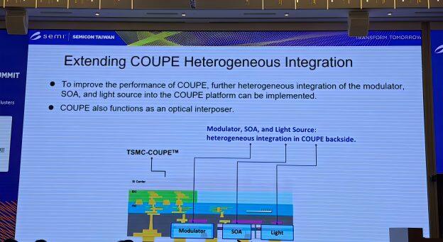
  TSMC is stepping up its technology roadmap to meet surging AI computing demand. According to TechNews, April Li, Global Head of AI and HPC Business Development at TSMC, said at SEMICON Taiwan 2026 that AI computing demand is growing fivefold annually, putting increasing pressure on compute capacity. In response, TSMC is integrating advanced process, 3DFabric, and silicon photonics into its HPC platform. Notably, the company expects SoIC and CoWoS integration to boost overall system computing performance to 50 times its 2024 level by 2029.  As the report indicates, Li said heterogeneous integration is the only way to push beyond current computing limits. TSMC plans N2P-on-N3P 3D integration in 2026, followed by A14-on-A14 in 2029, with interconnect pitch shrinking to 4.5 microns.  TSMC Advances COUPE and Silicon Photonics Design  TSMC is also continuing to advance its COUPE technology. According to TechNews, its 2–4-micron bonding pitch limits transmission loss at 112 Gbps to just 0.06 dB, compared with 1.38 dB for micro-bumps, helping reduce power consumption and latency to 10–20 nanoseconds.  As Mirror Daily indicates, TSMC’s self-developed COUPE platform uses TSMC-SoIC bonding technology to integrate electronic integrated circuits (EICs) with photonic integrated circuits (PICs), while supporting both grating couplers (GCs) and edge couplers (ECs). To further scale bandwidth, TSMC is pursuing two development paths. One will increase per-channel speeds from 200 Gbps to more than 400 Gbps while expanding channel counts from 16 to over 128, lifting total bandwidth from 3.2 Tbps to more than 12.8 Tbps. The other will expand wavelength-division multiplexing (WDM) from a single wavelength to 4, 8, 16, and beyond.  The company is also addressing testing and design challenges as CPO moves toward broader deployment. According to Mirror Daily, TSMC has enabled wafer-level optical testing for edge-coupled devices, allowing defective dies to be screened out before costly CPO assembly. TechNews adds that TSMC has introduced an optical PDK that enables electronic-photonic co-simulation to address key silicon photonics design challenges, while Mirror Media notes that the PDK supports Cadence and Synopsys tools to help accelerate product development.  Silicon Photonics Gains Ground as CPO Nears Mass Production  Beyond TSMC’s technology roadmap, silicon photonics is moving toward broader adoption and large-scale CPO deployment. As noted by Central News Agency, TSMC Vice President of Advanced Packaging Technology and Service K.C. Hsu said optical transceiver architectures are undergoing a structural shift, with silicon photonics expected to account for more than 50% of the optical transceiver market by 2027. CPO represents the next step, with some suppliers expected to begin mass production in the second half of 2026.  Hsu described optics as the “nervous system” of data centers as demand for high-speed connectivity grows. As noted by Central News Agency, he said optical transceiver sales rose 25% in 2025 and are expected to grow another 50% in 2026, while the high-end 100G-and-above market doubled in 2024 and expanded another 60% in 2025.  Hsu noted that Taiwan’s silicon foundry ecosystem is already capable of producing optical engines at scale and with high precision, while real-world data and market validation are helping ease longstanding concerns over CPO reliability. The bigger challenge to large-scale deployment now lies elsewhere in the supply chain, including lasers, optical fibers, fiber connectors, and product testing, he said, as reported by Central News Agency.
2026-09-01 15:44 阅读量:390
TSMC Arizona Profit Soars 663% YoY in 1H26; U.S. Earnings Pull Back 8.2% QoQ in 2Q as Depreciation Bites
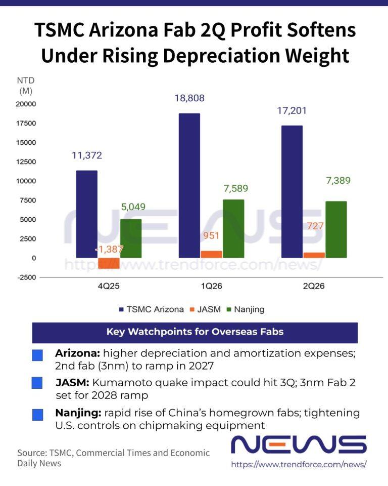
  As TSMC’s Arizona fabs ramp up to meet strong demand from NVIDIA and other Big Tech customers, the U.S. unit has overtaken TSMC Nanjing as the foundry giant’s most profitable overseas subsidiary. Citing TSMC’s 1H26 interim report, Commercial Times and the Economic Daily News report that TSMC Arizona posted a record NT$36.066 billion profit in 1H26, up 662.8% YoY.  As TSMC’s overseas footprint moves into a profit-harvesting phase, its four major manufacturing subsidiaries generated a combined NT$58.529 billion in 1H26, up 215.4% YoY. TSMC Arizona alone contributed more than 60% of the total, underscoring its growing weight in TSMC’s overseas earnings mix, as highlighted by the Economic Daily News.  Arizona Fab Profit Pulls Back QoQ as Depreciation Pressure Mounts  However, the Arizona profit surge showed signs of moderating in Q2. Its profit slipped 8.2% QoQ to NT$17.259 billion, even as it remained up a hefty 307.8% YoY, according to the Economic Daily News. Commercial Times further notes that TSMC recognized about NT$14.603 billion in investment income from its U.S. fab in the second quarter, down 13.6% from NT$16.909 billion in the first quarter.  Analysts cited by Commercial Times pointed out that as construction of subsequent fabs accelerates, higher depreciation and amortization expenses could put pressure on profitability.  TSMC has already warned that the overseas fab ramp-up will weigh on margins. CFO Wendell Huang said at the July earnings call that overseas expansion is expected to dilute gross margin by 2–3 percentage points in the early stages, widening to 3–4 points as the fabs mature.  As highlighted by Commercial Times, TSMC’s first Arizona fab entered 4nm mass production in 4Q24, while the second, focused on 3nm, is slated to ramp in 2H27. With the latest $100 billion investment, total planned U.S. investment has reached $265 billion, with the Arizona site ultimately expected to house 10 fabs and two advanced packaging facilities, according to MoneyDJ. How this aggressive expansion will impact profitability remains a key watchpoint.  Nanjing, JASM Profits Ease as Overseas Earnings Face New Tests  TSMC’s Nanjing fab remained a key profit driver, posting NT$14.978 billion in 1H26 and ranking second among its four major overseas operations. However, Q2 profit edged down to NT$7.389 billion from NT$7.589 billion in Q1, according to Economic Daily.  Meanwhile, JASM’s earnings also cooled slightly in Q2. As noted by Commercial Times, the Japan subsidiary, 73%-owned by TSMC, turned profitable this year after posting a loss in 2025, earning NT$951 million in Q1 and NT$727 million in Q2.  The bigger question now is whether JASM can keep that momentum after the July 7.1-magnitude Kumamoto earthquake. Commercial Times notes. The fab has resumed normal production and passed structural safety checks, but equipment requalification, calibration and wafer losses could reportedly weigh on Q3 results.
2026-08-18 11:25 阅读量:395
TSMC and Researchers Overcome 2D Semiconductor Bottleneck with Epitaxial Interface Engineering
  As conventional silicon semiconductor technology approaches its physical limits, 2D semiconductors are increasingly viewed as a key enabler for extending Moore’s Law. According to TechNews, citing Taiwan’s National Science and Technology Council (NSTC), a research team led by Dr. Iuliana Radu of TSMC, in collaboration with National Yang Ming Chiao Tung University (NYCU), has developed a high-performance monolayer molybdenum disulfide (MoS₂) top-gate transistor by addressing the long-standing interface challenges facing 2D semiconductors. The study was published in Nature Electronics.  The report explains that as silicon transistors approach their physical scaling limits, shrinking channel dimensions lead to higher leakage current and weaker electrostatic control. This has driven researchers to explore alternatives, with monolayer MoS₂ emerging as one of the most promising 2D semiconductor candidates. Despite its atomically thin structure, it retains semiconductor properties, making it well suited for smaller, more power-efficient transistors. However, 2D semiconductors require an ultrathin gate dielectric to control current flow, and depositing this layer often introduces dielectric-related scattering that degrades electron transport and device performance.  To overcome this challenge, the researchers focused not on discovering a new material, but on redesigning the interface through epitaxial interface engineering. Using ultra-high vacuum technology, the team first deposited an ultrathin aluminum layer onto monolayer MoS₂, then oxidized it to form an approximately 0.42nm-thick aluminum oxide (Al₂O₃) layer as a high-quality template for subsequent material growth. According to the report, this atomically thin interface improves the quality of the interface between the 2D semiconductor and the gate dielectric while reducing electron scattering, enabling both an ultrathin structure and high transconductance.  The resulting high-performance monolayer MoS₂ top-gate transistor delivers ultralow leakage current and excellent operational stability even at extremely small dimensions, the report says. By reconciling two long-standing tradeoffs—an ultrathin dielectric layer and high carrier mobility—the work demonstrates the practical potential of 2D semiconductor devices. According to the report, the technology could enable faster, lower-power electronic devices while integrating seamlessly with existing semiconductor manufacturing processes.  Leading Chipmakers Pursue 2D Transistor Technologies  TSMC has been advancing 2D-material transistor development. In June, TSMC, imec, and ASML unveiled a scalable 300mm integration route for 2D-material-based n-type field-effect transistors (nFETs) and p-type field-effect transistors (pFETs). According to an imec press release, the collaboration demonstrated, for the first time, 50nm contacted poly pitch (CPP) transistors using MoS₂, WS₂, and WSe₂ channel materials, establishing a manufacturing-compatible integration approach for next-generation 2D transistors.  Intel has also been advancing 2D transistor research. According to Tom’s Hardware, Intel Foundry and imec demonstrated a 300mm-ready integration of key process modules for 2D field-effect transistors (2DFETs) in late 2025. The collaboration featured a fab-compatible contact and gate-stack integration scheme, marking another step toward future manufacturing of 2D-material-based transistors. While commercialization remains a long-term goal, the work helps de-risk the development and eventual production of chips based on 2D materials.
2026-08-10 15:15 阅读量:441
  • 一周热料
  • 紧缺物料秒杀
型号 品牌 询价
RB751G-40T2R ROHM Semiconductor
CDZVT2R20B ROHM Semiconductor
MC33074DR2G onsemi
BD71847AMWV-E2 ROHM Semiconductor
TL431ACLPR Texas Instruments
型号 品牌 抢购
ESR03EZPJ151 ROHM Semiconductor
STM32F429IGT6 STMicroelectronics
IPZ40N04S5L4R8ATMA1 Infineon Technologies
BU33JA2MNVX-CTL ROHM Semiconductor
TPS63050YFFR Texas Instruments
BP3621 ROHM Semiconductor
热门标签
ROHM
Aavid
Averlogic
开发板
SUSUMU
NXP
PCB
传感器
半导体
相关百科
关于我们
AMEYA360微信服务号 AMEYA360微信服务号
AMEYA360商城(www.ameya360.com)上线于2011年,现 有超过3500家优质供应商,收录600万种产品型号数据,100 多万种元器件库存可供选购,产品覆盖MCU+存储器+电源芯 片+IGBT+MOS管+运放+射频蓝牙+传感器+电阻电容电感+ 连接器等多个领域,平台主营业务涵盖电子元器件现货销售、 BOM配单及提供产品配套资料等,为广大客户提供一站式购 销服务。

请输入下方图片中的验证码:

验证码