Intel Touts Auto AI Chip’s Efficiency

Release time:2017-12-01
author:Ameya360
source: Junko Yoshida
reading:1786

  Brian Krzanich, Intel’s CEO came to Los Angeles for the “AutoMobility LA” auto show flush with forecasts of how autonomous driving will change every aspect of future vehicles, from cabin design to entertainment and life-saving safety systems.

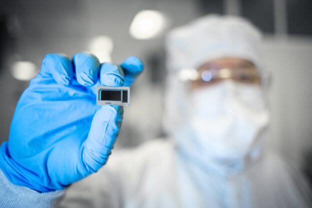
  As a leading autonomous vehicle chip company, Intel also seized the moment to set the record straight on the efficiency of the EyeQ 5 chip, developed by Mobileye (now an Intel company), compared to Nvidia’s Drive PX Xavier SoC designed for autonomous driving.

  During his speech, Krzanich, referring to the recently completed Mobileye acquisition, stressed that Intel “can deliver more than twice the deep-learning performance efficiency than the competition [meaning Nvidia].”

  As Nvidia strives to brand itself as a leader in AI-based autonomous driving technology through relentless promotion of its Drive PX platform, Intel appears to have decided to charge full-tilt into the brewing battle of specsmanship.

  Incorrectly quoted

  Speaking with EE Times, Jack Weast, Intel's principal engineer and chief architect of autonomous driving solutions, described Intel as a company that tends to lean conservative when it comes to touting its chips’ performance. As the war of words escalates, though, Weast said, “We are tired of seeing us incorrectly quoted.”

  Weast complained that its rivals and the media often incorrectly compared Nvidia’s Drive PX to Intel’s desktop PC chips. In an apple-to-apple comparison, Mobileye’s 5th generation vision-sensor fusion chip must instead be compared, he said, with Nvidia’s Xavier SoC. EyeQ5 delivers 24 trillion operations per second (TOPS) at 10 watts, Weast said. In contrast, the DRIVE PX Xavier offers 30 TOPS of performance, while consuming 30 watts of power. “We are 2.4 times more efficient,” said Weast.

  Of course, Nvidia is now promoting its latest Pegasus SoC, scheduled for delivery in 2018, designed to perform 320 TOPS — more than 10x the performance of its predecessor — at 500 watts of power. “Pegasus is new, but its efficiency isn’t getting better,” Weast said.

  Nvidia’s Pegasus couples two of NVIDIA's Xavier SoCs with two next-generation discrete GPUs with hardware acceleration.

  The mystery that remains, even to some experts, is how Intel plans to combine Mobileye’s “eye” with an Intel microprocessor “brain” in a highly automated vehicle.

  Intel, in fact, might partly share the blame for the market’s confusion. The CPU giant has remained silent about what sort of SoCs it’s been developing on its own, separate from Mobileye’s EyeQ5.

  Intel to launch multi-chip platform

  According to Weast, Intel is planning to unveil soon — leading up to the Consumer Electronics Show in January — “a multi-chip platform for autonomous driving.” The solution will combine the EyeQ 5 SoC, Intel’s low-power Atom SoCs, and other hardware including I/O and Ethernet connectivity, he explained.

  When Intel unveiled its GO development platform for autonomous driving earlier this year, it described its Atom processor C3000 as a chip that “delivers high performance per watt, packing substantial compute into low-power designs.”

  Asked how the Atom SoC shares processing tasks with EyeQ 5, Weast said, “We looked at the entire set of workload necessary for autonomous vehicles.” Then, he said, “We allocated and partitioned the compute loads” among multiple chips.

  Asked if FPGA is a part of that multi-chip solution, Weast said no. “There are some customers looking at FPGAs for certain applications such custom I/O or security, but it’s not part of our new multi-chip platform.”

  Division of labor

  When Mobileye originally announced EyeQ 5 before being acquired by Intel, the Israeli company touted the new SoC as a “brain” of autonomous vehicles, tasked to do “the vision central computer performing sensor fusion” for fully autonomous driving (Level 5) vehicles.

  If so, where does Intel’s Atom SoC come in?

  Autonomous driving requires different levels of sensor fusion, Weast explained. In deep-learning acceleration, some sensor fusion demands a chip to process highly parallel multi-threaded chunks of codes. “For that, EyeQ 5 is ideal.” Meanwhile, there is also a need for higher-level, environmental sensor fusion, which looks at trajectories and validations, Weast explained. “A CPU is a better fit to perform such tasks.”

  In Intel’s view, Weast said, in enabling highly automated driving, “We didn’t have to cram everything into one SoC, such as EyeQ 5.” Intel had “the luxury of an opportunity to figure out where the spare cycle is, and how the compute workload should be partitioned,” he explained.

  As soon as the Mobileye deal was completed last August, everyone on the team “immediately dove into the project,” Weast said.

  Intel will shortly detail its multi-chip platform designed for autonomous driving, Weast promised. “At that point, we should be able to offer a platform-level comparison” between Nvidia’s Drive PX and Intel’s solution, he said.

("Note: The information presented in this article is gathered from the internet and is provided as a reference for educational purposes. It does not signify the endorsement or standpoint of our website. If you find any content that violates copyright or intellectual property rights, please inform us for prompt removal.")

Online messageinquiry

reading
Intel Patent Reveals XBM Matching HBM4 Footprint Without Interposers; Commercialization Seen After 2030
  As AI chip demand surges, existing high-bandwidth memory (HBM) is facing supply and cost challenges, prompting the search for alternative memory technologies. According to Tom’s Hardware, an Intel patent application published on July 2, 2026 reveals the company’s proposed cross-batch memory (XBM) architecture, designed to ease the packaging and cost bottlenecks of today’s interposer-based HBM. The report states that the design aims to match HBM4’s footprint while replacing conventional DRAM and its ultra-wide interface with back-end-of-line (BEOL) transistors and serial Universal Chiplet Interconnect Express (UCIe) links.  As noted by Wccftech, XBM is expected to target commercialization after 2030, in line with ZAM, the memory architecture Intel is co-developing with SoftBank subsidiary SAIMEMORY.  XBM Architecture and Advantages  The proposed architecture centers on DRAM blocks connected to a UCIe I/O block operating at 32 GT/s, with the I/O routed through the base die. According to Wccftech, each XBM stack provides a die capacity ranging from 0.5GB to 5GB. Each sub-channel consists of 12 data blocks, with up to 96 data blocks in an 8-high XBM stack and 192 in a 16-high stack. These channels operate at 2GHz. The report also notes that XBM can be implemented in multiple package configurations, including Memory-on-Package (MoP), enabling higher bandwidth and capacity in smaller form-factor designs.  Notably, the memory die uses 1T1C (one transistor, one capacitor) back-end DRAM, with transistors fabricated in the back-end-of-line (BEOL) metal layers rather than front-end silicon, Wccftech says. According to the report, this significantly improves area efficiency, allowing more space for TSVs (Through-Silicon Via) and enabling higher memory density and bandwidth.  Competitive and Ecosystem Challenges  The global HBM market is currently dominated by South Korean suppliers. As Global Economic News points out, conventional HBM incurs high manufacturing costs due to the micro-bump processes used to vertically stack DRAM dies, while silicon interposers add significant routing complexity and cost. Intel’s proposed XBM architecture is designed to address these limitations.  However, Global Economic News also notes that Intel’s proposal is unlikely to immediately shift the industry’s competitive landscape. SK hynix and Samsung Electronics have spent several years developing cost-saving technologies, including standard chiplets, UCIe, and fan-out packaging, to reduce interposer costs. The report further notes that platform compatibility and software ecosystems remain major barriers to adoption. The global AI accelerator ecosystem, led by NVIDIA, is currently optimized for the existing HBM architecture and wide-bandwidth parallel interfaces, making a transition to alternative memory architectures more challenging.
2026-07-09 11:24 reading:354
Intel Reportedly Weighs Dual-Side Power Delivery for 14A2 to Boost Chip Density in Race With TSMC, Samsung
  Intel is reportedly refining its 1.4nm roadmap with a new power delivery architecture. According to ETNews, sources say the company originally planned to rely exclusively on its PowerDirect back-side power delivery network (BSPDN) for the baseline 14A node. However, Intel is now reportedly considering a dual-side architecture for the follow-on 14A2 process that combines both front-side and back-side power delivery.  The report says the architectural change is driven by lithography limitations as Intel pushes the pitch of its lowest metal layer (M0) to around 21nm, where stochastic defects become increasingly difficult to manage.  Intel has previously said it aims to increase chip density by 1.3× over 18A to compete with TSMC’s N2/A14 and Samsung’s SF2Z. While 14A targets an M0 pitch of approximately 28nm, industry analysis cited by the report suggests the follow-on 14A2 could reduce it to around 21nm. The report says the resulting density gains would help justify the use of High-NA EUV lithography systems, despite requiring double patterning, which cost hundreds of billions of Korean won.  The challenge, however, is that shrinking circuit lines below 21nm causes interconnect resistance to rise exponentially. The report says the nano Through-Silicon Via (nTSV) infrastructure built for back-side power delivery alone may no longer meet the current density requirements of the transistors, leading to severe IR drop, or voltage loss. Intel is therefore expected to keep the back-side power delivery network as the primary power path while repurposing portions of the front-side metal layers to carry supplemental power and clock signals.  The report says the hybrid architecture is a design compromise aimed at preserving sufficient power margin as Intel pushes toward more aggressive scaling while confronting lithography limitations. Although it adds routing complexity, the approach is viewed as necessary to achieve the targeted 21nm M0 pitch.  Intel’s reported move also comes as TSMC advances its Super Power Rail (SPR) backside power delivery roadmap, with A16 slated for volume production in 2027 and A12 targeted for 2029, both incorporating the technology for AI and HPC applications, according to Tom’s Hardware.  Roadmap Comparison  The ETNews report also highlights Intel’s tight development timeline. According to its roadmap, the 14A process is scheduled to enter risk production in 2028, followed by volume production in 2029. Intel is also expected to distribute version 0.9 of its 14A Process Design Kit (PDK) to external customers in October, the report adds.  By the time Intel reaches risk production, however, TSMC is expected to already be shipping commercial products built on its A14 process. The report notes that TSMC had already achieved stable yields on its N2 process during 2025–2026 and entered the market in line with Apple’s product launch schedule. As for Samsung, The Elec reports that the company has recently reaffirmed plans to begin mass production of its 1.4nm process in 2029, followed by the enhanced SF1.4+ node in 2030.
2026-07-07 11:21 reading:393
Intel Taps SK hynix Ex-CEO as Foundry EVP to Lead Advanced Packaging Push as EMIB, HBI Scale Up
  Intel CEO Lip-Bu Tan is accelerating the company’s foundry ambitions, continuing to recruit seasoned talent from across the chip industry. The latest move is the appointment of Seok-Hee Lee as Executive Vice President of Intel Foundry, according to an Intel announcement on June 18.  Notably, Lee joins Intel after serving as president and CEO of SK On and previously leading SK hynix. A semiconductor industry veteran, he also held engineering leadership roles at Intel and in academia, bringing deep expertise in advanced process technologies and large-scale manufacturing, according to the press release.  Reporting directly to Tan, Lee will oversee advanced packaging, system integration, back-end technology development, and manufacturing, as noted by the company. Intel said the appointment is aimed at strengthening its system-level innovation capabilities and supporting the next phase of its foundry expansion.  Tan also underscored Lee’s pivotal role in advancing Intel’s next-generation packaging strategy.“As we prepare to scale advanced packaging technologies, including EMIB-T and HBI, for high-volume production, Seok-Hee is the ideal leader to drive the growth of this strategically important business,” Tan said.  The appointment, as Reuters points out, comes after U.S. President Donald Trump announced earlier that Apple had agreed to collaborate with Intel on designing and manufacturing chips in the United States, providing a potential boost to Intel’s foundry business.  A previous Reuters report, citing The Information, also reported that Google has tapped Intel to manufacture more than 3 million TPUs in 2028, while NVIDIA is evaluating Intel’s 18A process and advanced packaging technologies for a next-generation multi-die GPU design.  Meanwhile, Intel Foundry EVP Naga Chandrasekaran will continue reporting to CEO Lip-Bu Tan, overseeing front-end technology development and manufacturing as Intel accelerates the ramp of Intel 18A, Intel 14A and future process nodes. He will also retain responsibility for design enablement and customer-facing business operations, supporting Intel Foundry’s long-term growth.  Intel’s Talent Offensive Continues  Lee’s appointment marks the latest in a series of high-profile hires since Lip-Bu Tan took the helm at Intel. Reuters notes that the company bolstered its foundry ambitions in April by recruiting Samsung foundry veteran Shawn Han to support its contract manufacturing business.  The hiring drive began earlier. In late 2025, Intel brought in former TSMC senior vice president Wei-Ren Lo as executive vice president overseeing manufacturing and packaging amid controversy surrounding alleged sub-2nm trade secrets. Intel said Lo’s return was part of its broader transformation effort, with the veteran executive bringing back nearly two decades of experience gained at Intel before joining TSMC.
2026-06-22 10:51 reading:435
Intel Says 18A May Reach Strong Margins by 2027; Notebook Chips on the Node Mark Fastest Ramp in 5 Years
  Intel is betting heavily on 18A to support the company’s turnaround plan. According to The Register, Chief Financial Officer David Zinsner said that early last year Intel faced the challenge of trying to improve both performance and yield at the same time. The company later shifted its focus to stabilizing performance first, and with that objective largely achieved, it is now concentrating on improving yield month by month.  Zinsner said Intel’s goal is to achieve yield levels that support strong margins, adding that the company is currently ahead of schedule to reach that target by the end of 2027, as the report highlights. He added that after Lip-Bu Tan joined the company, Intel began sharing more manufacturing data with its vendors. The increased collaboration helped improve yields and made a dramatic difference.  Looking beyond 18A, Zinsner also expressed confidence in Intel’s 14A. According to the report, he said the company has adopted a more aggressive approach than it did with 18A, adding that yield and performance metrics are currently ahead of where 18A was at the same stage of development.  Intel 3 and 18A Supply Set to Rise Amid Strong CPU Demand  In addition to providing an update on Intel’s manufacturing roadmap, Zinsner highlighted growing supply from Intel 3 and 18A, according to Seeking Alpha. As cited by the report, he said Intel expects a meaningful increase in supply from both Intel 3 and 18A over the coming quarters to meet rising demand. He added that 18A-based notebook processors are ramping quickly and represent the company’s fastest-ramping product launch in at least the past five years.  The company is also seeing rising CPU demand. According to The Register, Zinsner said it remains difficult to predict the full extent of future growth, but he expects the market to be substantial. He said the key challenge at present is supply, adding that Intel sees sufficient demand in the market and should be able to grow data center revenue meaningfully if it executes successfully on planned supply ramps.
2026-06-05 10:40 reading:646
  • Week of hot material
  • Material in short supply seckilling
model brand Quote
BD71847AMWV-E2 ROHM Semiconductor
TL431ACLPR Texas Instruments
CDZVT2R20B ROHM Semiconductor
MC33074DR2G onsemi
RB751G-40T2R ROHM Semiconductor
model brand To snap up
ESR03EZPJ151 ROHM Semiconductor
TPS63050YFFR Texas Instruments
IPZ40N04S5L4R8ATMA1 Infineon Technologies
STM32F429IGT6 STMicroelectronics
BP3621 ROHM Semiconductor
BU33JA2MNVX-CTL ROHM Semiconductor
Hot labels
ROHM
IC
Averlogic
Intel
Samsung
IoT
AI
Sensor
Chip
About us

Qr code of ameya360 official account

Identify TWO-DIMENSIONAL code, you can pay attention to

AMEYA360 weixin Service Account AMEYA360 weixin Service Account
AMEYA360 mall (www.ameya360.com) was launched in 2011. Now there are more than 3,500 high-quality suppliers, including 6 million product model data, and more than 1 million component stocks for purchase. Products cover MCU+ memory + power chip +IGBT+MOS tube + op amp + RF Bluetooth + sensor + resistor capacitance inductor + connector and other fields. main business of platform covers spot sales of electronic components, BOM distribution and product supporting materials, providing one-stop purchasing and sales services for our customers.

Please enter the verification code in the image below:

verification code