TSMC Tips 7+, 12, 22nm Nodes

发布时间:2017-03-14 00:00
作者:Ameya360
来源:EE TIMES
阅读量:5961

  Trying to cover the waterfront, TSMC disclosed plans for new high-, mid- and low-end processes at an annual event here. They included an enhanced 7nm FinFET node using extreme ultraviolet lithography, a 12nm upgrade of its 16nm process and a 22nm planar technology — its answer to fully depleted silicon-on-insulator (FD-SOI).

  The foundry also described enhancements to its two chip-stacking techniques, advances in RF CMOS and work in transistors and materials, paving the way to a 3nm node and beyond. In addition, it previewed design capabilities using machine learning that it will offer before the end of the year.

  Among its achievements, TSMC noted 76 percent yields on the 256Mbit SRAM made in its first-generation 7nm node, which will be in volume production next year. It also reported that an ARM Cortex-A72 processor in the node exceeded 4GHz using a new design flow.

  The proliferation of different nodes, sub-nodes and platforms threatens to create a dizzying array of options. TSMC has clearly focused on easing migrations for designers, sometimes at the expense of advances measured in single digits.

  The Taiwan company, already the world’s largest foundry by far, expects to ship 11 million 12-inch-equivalent wafers this year, a typical 10 percent annual increase. The biggest share—two million wafers—will use its planar 28nm processes for which it is boosting capacity 15 percent this year.

  TSMC has taped out nearly 800 chips using flavors of its 28nm process. It has shipped 4.5 million 28nm wafers to date, clearly a big sweet spot it aims to defend.

  Globalfoundries hopes to capture many of those customers starting this year with 22nm FD-SOI, a lower cost, lower power alternative with similar performance to TSMC’s 16nm FinFET node. TSMC claims its 22nm process provides an easier migration path from 28nm while FD-SOI requires redesigned intellectual property cores.

  “Bulk semiconductor technology has been enhanced for 30 years and is used by Intel and Samsung,” the world’s two largest chip makers, said Mark Liu, TSMC’s co-chief executive in a brief interview after a keynote here. “FD-SOI will always be the technology of the future,” he quipped.

  The news comes the same day NXP announced it will use FD-SOI for multiple future processors. So far, a total of just 10,000 FD-SOI wafers/month are shipping from all fabs including Globalfoundries and STMicroelectronics, said Sam Wang, a chip analyst for Gartner.

  Globalfoundries may be slightly ahead in timing, ramping its 22nm FD-SOI process now with Sony image sensors in production. TSMC said its 22nm process will be in production next year, aimed at 5G RF and other mobile chips including image processors and components for wearables and the Internet of Things.

  The 22nm FD-SOI node sports similar specs to TSMC’s 22nm process, “but it does not have the comprehensive IP ecosystem… and the manufacturing track record we have,” said B.J. Woo, vice president of business development at TSMC.

  TSMC also plans an ultra-low power version of its 12nm FinFET process, supporting 0.5V operation and starting risk production before June. It will likely be positioned as a competitor to the 12nm FD-SOI process Globalfoundries announced last year but is not expected in production until 2019.

  The ultra-low power TSMC 22nm process should deliver a 20 percent area shrink and either 0.45x the power or 1.32x the speed of its 28 HPM process, Woo said. Compared to its 28 HPC+ process, the 22nm is a direct optical shrink with better transistors and 0.6 Vdd operation offering 10 percent smaller size and 35 percent less power or 15 percent more speed, she said.

  TSMC’s 22nm node uses the same mask counts, design rules, SRAM bit cells and I/O devices as its 28HPC+ node. Designers only need to adopt its boosted transistors and re-characterize foundation IP to ensure they meet new margins, Woo said.

  “The migration effort is really different [from FD-SOI]—it’s a day and night difference,” said Jack Sun, a vice president of R&D at TSMC.

  TSMC’s Liu said the foundry expects 70 tape outs of IoT chips this year across its family of ultra-low power processes that range from 55 to 28nm. The 40nm ULP process has been characterized for near-threshold operation driving energy efficiency to 11 microamps/MHz, he said.

(备注:文章来源于网络,信息仅供参考,不代表本网站观点,如有侵权请联系删除!)

在线留言询价

相关阅读
TSMC Arizona Profit Soars 663% YoY in 1H26; U.S. Earnings Pull Back 8.2% QoQ in 2Q as Depreciation Bites
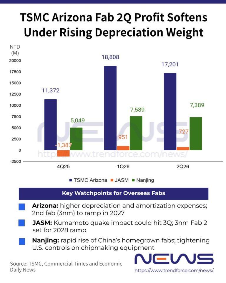
  As TSMC’s Arizona fabs ramp up to meet strong demand from NVIDIA and other Big Tech customers, the U.S. unit has overtaken TSMC Nanjing as the foundry giant’s most profitable overseas subsidiary. Citing TSMC’s 1H26 interim report, Commercial Times and the Economic Daily News report that TSMC Arizona posted a record NT$36.066 billion profit in 1H26, up 662.8% YoY.  As TSMC’s overseas footprint moves into a profit-harvesting phase, its four major manufacturing subsidiaries generated a combined NT$58.529 billion in 1H26, up 215.4% YoY. TSMC Arizona alone contributed more than 60% of the total, underscoring its growing weight in TSMC’s overseas earnings mix, as highlighted by the Economic Daily News.  Arizona Fab Profit Pulls Back QoQ as Depreciation Pressure Mounts  However, the Arizona profit surge showed signs of moderating in Q2. Its profit slipped 8.2% QoQ to NT$17.259 billion, even as it remained up a hefty 307.8% YoY, according to the Economic Daily News. Commercial Times further notes that TSMC recognized about NT$14.603 billion in investment income from its U.S. fab in the second quarter, down 13.6% from NT$16.909 billion in the first quarter.  Analysts cited by Commercial Times pointed out that as construction of subsequent fabs accelerates, higher depreciation and amortization expenses could put pressure on profitability.  TSMC has already warned that the overseas fab ramp-up will weigh on margins. CFO Wendell Huang said at the July earnings call that overseas expansion is expected to dilute gross margin by 2–3 percentage points in the early stages, widening to 3–4 points as the fabs mature.  As highlighted by Commercial Times, TSMC’s first Arizona fab entered 4nm mass production in 4Q24, while the second, focused on 3nm, is slated to ramp in 2H27. With the latest $100 billion investment, total planned U.S. investment has reached $265 billion, with the Arizona site ultimately expected to house 10 fabs and two advanced packaging facilities, according to MoneyDJ. How this aggressive expansion will impact profitability remains a key watchpoint.  Nanjing, JASM Profits Ease as Overseas Earnings Face New Tests  TSMC’s Nanjing fab remained a key profit driver, posting NT$14.978 billion in 1H26 and ranking second among its four major overseas operations. However, Q2 profit edged down to NT$7.389 billion from NT$7.589 billion in Q1, according to Economic Daily.  Meanwhile, JASM’s earnings also cooled slightly in Q2. As noted by Commercial Times, the Japan subsidiary, 73%-owned by TSMC, turned profitable this year after posting a loss in 2025, earning NT$951 million in Q1 and NT$727 million in Q2.  The bigger question now is whether JASM can keep that momentum after the July 7.1-magnitude Kumamoto earthquake. Commercial Times notes. The fab has resumed normal production and passed structural safety checks, but equipment requalification, calibration and wafer losses could reportedly weigh on Q3 results.
2026-08-18 11:25 阅读量:215
TSMC and Researchers Overcome 2D Semiconductor Bottleneck with Epitaxial Interface Engineering
  As conventional silicon semiconductor technology approaches its physical limits, 2D semiconductors are increasingly viewed as a key enabler for extending Moore’s Law. According to TechNews, citing Taiwan’s National Science and Technology Council (NSTC), a research team led by Dr. Iuliana Radu of TSMC, in collaboration with National Yang Ming Chiao Tung University (NYCU), has developed a high-performance monolayer molybdenum disulfide (MoS₂) top-gate transistor by addressing the long-standing interface challenges facing 2D semiconductors. The study was published in Nature Electronics.  The report explains that as silicon transistors approach their physical scaling limits, shrinking channel dimensions lead to higher leakage current and weaker electrostatic control. This has driven researchers to explore alternatives, with monolayer MoS₂ emerging as one of the most promising 2D semiconductor candidates. Despite its atomically thin structure, it retains semiconductor properties, making it well suited for smaller, more power-efficient transistors. However, 2D semiconductors require an ultrathin gate dielectric to control current flow, and depositing this layer often introduces dielectric-related scattering that degrades electron transport and device performance.  To overcome this challenge, the researchers focused not on discovering a new material, but on redesigning the interface through epitaxial interface engineering. Using ultra-high vacuum technology, the team first deposited an ultrathin aluminum layer onto monolayer MoS₂, then oxidized it to form an approximately 0.42nm-thick aluminum oxide (Al₂O₃) layer as a high-quality template for subsequent material growth. According to the report, this atomically thin interface improves the quality of the interface between the 2D semiconductor and the gate dielectric while reducing electron scattering, enabling both an ultrathin structure and high transconductance.  The resulting high-performance monolayer MoS₂ top-gate transistor delivers ultralow leakage current and excellent operational stability even at extremely small dimensions, the report says. By reconciling two long-standing tradeoffs—an ultrathin dielectric layer and high carrier mobility—the work demonstrates the practical potential of 2D semiconductor devices. According to the report, the technology could enable faster, lower-power electronic devices while integrating seamlessly with existing semiconductor manufacturing processes.  Leading Chipmakers Pursue 2D Transistor Technologies  TSMC has been advancing 2D-material transistor development. In June, TSMC, imec, and ASML unveiled a scalable 300mm integration route for 2D-material-based n-type field-effect transistors (nFETs) and p-type field-effect transistors (pFETs). According to an imec press release, the collaboration demonstrated, for the first time, 50nm contacted poly pitch (CPP) transistors using MoS₂, WS₂, and WSe₂ channel materials, establishing a manufacturing-compatible integration approach for next-generation 2D transistors.  Intel has also been advancing 2D transistor research. According to Tom’s Hardware, Intel Foundry and imec demonstrated a 300mm-ready integration of key process modules for 2D field-effect transistors (2DFETs) in late 2025. The collaboration featured a fab-compatible contact and gate-stack integration scheme, marking another step toward future manufacturing of 2D-material-based transistors. While commercialization remains a long-term goal, the work helps de-risk the development and eventual production of chips based on 2D materials.
2026-08-10 15:15 阅读量:274
TSMC’s June Revenue Hits Record NT$442.7 Billion, Q2 Sales Reach Guidance High End: Earnings Call Preview
  Ahead of TSMC’s July 16 earnings call, the foundry giant today posted record June sales, with revenue rising 6.2% MoM and 67.9% YoY to reach NT$442.7 billion, according to its press release. The strong June performance lifted TSMC’s Q2 revenue to approximately NT$1.27 trillion, falling on the upper end its original guidance range of US$39 billion–$40.2 billion (roughly equivalent to NT$1.24 trillion–NT$1.27 trillion) and marking a new quarterly record.  TSMC’s cumulative revenue for January through June 2026 reached NT$2,404,484 million, up 35.6% year-on-year from NT$1,773,046 million in the same period of 2025, the company said.  Upside Ahead for 2026 Revenue and Q2 Gross Margin  Against the backdrop of stronger-than-expected June sales, analysts cited by Commercial Times expect TSMC to also outperform its 2026 full-year revenue outlook and Q2 gross margin guidance. The company previously guided for full-year U.S. dollar revenue growth of above 30%, but Morgan Stanley now expects the company to raise the outlook toward 40% YoY, while UBS has lifted its forecast to 37%, according to the report.  For profitability, analysts also see upside to TSMC’s Q2 gross margin guidance of 65.5%–67.5%, with some brokerages cited by Commercial Times forecasting margins approaching 70%, including estimates of 69% and 69.5%.  Looking further ahead, Liberty Times, citing analysts, expects TSMC’s margin momentum to remain strong through 2027, with gross margin projected to stay above 66% this year and exceed 68% next year.  Aggressive Capex Push Ahead  Meanwhile, TSMC is expected to step up its investment pace, with analysts seeing further upside beyond the company’s 2026 capex guidance. While TSMC expects 2026 capital spending to land at the high end of its US$52 billion–$56 billion range, analysts cited by Commercial Times expect faster 2nm and 3nm expansion to push capex higher, with forecasts reaching US$58 billion and even US$60 billion from more bullish estimates.  The aggressive spending plan is expected to fuel TSMC’s advanced-node expansion. Economic Daily News, citing analysts, expects 3nm capacity to reach 170,000 wafers per month this year and surpass 200,000 by 2028. Combined A14, 2nm/A16, and 3nm capacity could reach 350,000–400,000 wafers per month, the report adds.  The investment push is also expected to extend into advanced packaging. Commercial Times, citing analysts, forecasts TSMC’s CoWoS capacity to reach 2 million units by 2027, significantly above the previous estimate of 1.35 million. Notably, the Economic Daily News highlights that TSMC’s CoPoS is expected to enter mass production in 2029–2030, with initial capacity of 40,000–50,000 wafers per month.
2026-07-14 15:23 阅读量:563
TSMC Rejects High-NA EUV Investment Concerns, Confirms Purchase for R&D Use
  As Intel advances its High-NA EUV roadmap for its A14 node, market attention has turned to TSMC’s comparatively cautious approach to the cutting-edge lithography tool, which is estimated to cost around US$400 million per system.  However, at its June 4 shareholder meeting, TSMC Chairman C.C. Wei rejected speculation that the company had opted not to invest in High-NA EUV. According to TechNews, he stressed that TSMC has already purchased the equipment and is actively conducting R&D.  Wei explained that the main reason the High-NA EUV system has not yet been introduced into mass production is purely cost-related. The company will continue working to improve efficiency and reduce costs, and will move the technology into production once conditions are ready, TechNews reports.  Interestingly, Wei also added with a touch of humor that TSMC is not only investing in the technology but has already purchased the tools, noting that “it would even be a bit embarrassing to say how many.” As previously reported by Tom’s Hardware, citing Kevin Zhang, senior vice president of business development and global sales and deputy COO at TSMC, TSMC’s upcoming A13 and A12 processes, both targeted for 2029, are not expected to require High-NA EUV lithography tools.  This contrasts with Intel’s strategy for its 14A node and subsequent generations, which are set to adopt High-NA EUV starting in 2027–2028, according to Tom’s Hardware. Reuters, citing ASML CEO Christophe Fouquet, also reported in May that the semiconductor equipment giant expects to see the first memory and logic products manufactured on High-NA EUV systems within the next few months.  TSMC Reaffirms Strong Capex Outlook  Against this backdrop, TSMC reaffirmed its capital expenditure plans to support sustained growth. According to TechNews, when investors asked Chairman C.C. Wei how long the company’s current investment cycle would last and when a potential “plateau period” might emerge, he said TSMC remains highly confident in its multi-year outlook, supported by forecasts from both customers and “customers’ customers,” with the company’s growth trajectory expected to continue upward.  He noted that, as previously guided at the earnings call, capital expenditure for 2026 is projected to range between US$52 billion and US$56 billion, with an internal bias toward the upper end of US$56 billion, as noted by the report.  Liberty Times adds that at TSMC’s annual shareholder meeting, C.C. Wei said in his opening remarks that the company achieved record-high revenue and profit last year, delivering strong operational results. He noted that TSMC’s share price has risen by more than 1.5 times over the past year, while cash dividend payouts have increased by over 30%.
2026-06-05 10:44 阅读量:926
  • 一周热料
  • 紧缺物料秒杀
型号 品牌 询价
TL431ACLPR Texas Instruments
RB751G-40T2R ROHM Semiconductor
BD71847AMWV-E2 ROHM Semiconductor
CDZVT2R20B ROHM Semiconductor
MC33074DR2G onsemi
型号 品牌 抢购
STM32F429IGT6 STMicroelectronics
IPZ40N04S5L4R8ATMA1 Infineon Technologies
BP3621 ROHM Semiconductor
TPS63050YFFR Texas Instruments
ESR03EZPJ151 ROHM Semiconductor
BU33JA2MNVX-CTL ROHM Semiconductor
热门标签
ROHM
Aavid
Averlogic
开发板
SUSUMU
NXP
PCB
传感器
半导体
相关百科
关于我们
AMEYA360微信服务号 AMEYA360微信服务号
AMEYA360商城(www.ameya360.com)上线于2011年,现 有超过3500家优质供应商,收录600万种产品型号数据,100 多万种元器件库存可供选购,产品覆盖MCU+存储器+电源芯 片+IGBT+MOS管+运放+射频蓝牙+传感器+电阻电容电感+ 连接器等多个领域,平台主营业务涵盖电子元器件现货销售、 BOM配单及提供产品配套资料等,为广大客户提供一站式购 销服务。

请输入下方图片中的验证码:

验证码