TSMC 7-nm Process Experiencing Heavy Market Demand

Release time:2018-07-25
author:Ameya360
source:CTIMES
reading:1599

Taiwan Semiconductor Manufacturing Company, Limited (TSMC) last Thursday at a legal briefing stated that their 7-nm chip process has already gone into mass production. They estimate that during the third quarter it will account for 10% of their revenue and then increase to account for 20% of their revenue in the fourth quarter.

TSMC 7-nm Process Experiencing Heavy Market Demand

TSMC CEO and Vice Chairman C.C. Wei stated that currently 7-nm has already gone into mass production and can be used in servers, AP, CPU, and GPU; furthermore, it is expected to contribute to 10% of TSMC’s revenue. He also pointed out that increased demand for high-speed computers and high-end mobile phones will be the main sources of growth in the third quarter.

In addition, the design for EUV equipment which uses 7 + nm was also finalized this month, and they expect to finalize more designs at the end of this year with the processes formally going into mass production in the second quarter of 2019. Following that, 5-nm processes will also be introduced for EUV.

("Note: The information presented in this article is gathered from the internet and is provided as a reference for educational purposes. It does not signify the endorsement or standpoint of our website. If you find any content that violates copyright or intellectual property rights, please inform us for prompt removal.")

Online messageinquiry

reading
TSMC’s June Revenue Hits Record NT$442.7 Billion, Q2 Sales Reach Guidance High End: Earnings Call Preview
  Ahead of TSMC’s July 16 earnings call, the foundry giant today posted record June sales, with revenue rising 6.2% MoM and 67.9% YoY to reach NT$442.7 billion, according to its press release. The strong June performance lifted TSMC’s Q2 revenue to approximately NT$1.27 trillion, falling on the upper end its original guidance range of US$39 billion–$40.2 billion (roughly equivalent to NT$1.24 trillion–NT$1.27 trillion) and marking a new quarterly record.  TSMC’s cumulative revenue for January through June 2026 reached NT$2,404,484 million, up 35.6% year-on-year from NT$1,773,046 million in the same period of 2025, the company said.  Upside Ahead for 2026 Revenue and Q2 Gross Margin  Against the backdrop of stronger-than-expected June sales, analysts cited by Commercial Times expect TSMC to also outperform its 2026 full-year revenue outlook and Q2 gross margin guidance. The company previously guided for full-year U.S. dollar revenue growth of above 30%, but Morgan Stanley now expects the company to raise the outlook toward 40% YoY, while UBS has lifted its forecast to 37%, according to the report.  For profitability, analysts also see upside to TSMC’s Q2 gross margin guidance of 65.5%–67.5%, with some brokerages cited by Commercial Times forecasting margins approaching 70%, including estimates of 69% and 69.5%.  Looking further ahead, Liberty Times, citing analysts, expects TSMC’s margin momentum to remain strong through 2027, with gross margin projected to stay above 66% this year and exceed 68% next year.  Aggressive Capex Push Ahead  Meanwhile, TSMC is expected to step up its investment pace, with analysts seeing further upside beyond the company’s 2026 capex guidance. While TSMC expects 2026 capital spending to land at the high end of its US$52 billion–$56 billion range, analysts cited by Commercial Times expect faster 2nm and 3nm expansion to push capex higher, with forecasts reaching US$58 billion and even US$60 billion from more bullish estimates.  The aggressive spending plan is expected to fuel TSMC’s advanced-node expansion. Economic Daily News, citing analysts, expects 3nm capacity to reach 170,000 wafers per month this year and surpass 200,000 by 2028. Combined A14, 2nm/A16, and 3nm capacity could reach 350,000–400,000 wafers per month, the report adds.  The investment push is also expected to extend into advanced packaging. Commercial Times, citing analysts, forecasts TSMC’s CoWoS capacity to reach 2 million units by 2027, significantly above the previous estimate of 1.35 million. Notably, the Economic Daily News highlights that TSMC’s CoPoS is expected to enter mass production in 2029–2030, with initial capacity of 40,000–50,000 wafers per month.
2026-07-14 15:23 reading:332
TSMC Rejects High-NA EUV Investment Concerns, Confirms Purchase for R&D Use
  As Intel advances its High-NA EUV roadmap for its A14 node, market attention has turned to TSMC’s comparatively cautious approach to the cutting-edge lithography tool, which is estimated to cost around US$400 million per system.  However, at its June 4 shareholder meeting, TSMC Chairman C.C. Wei rejected speculation that the company had opted not to invest in High-NA EUV. According to TechNews, he stressed that TSMC has already purchased the equipment and is actively conducting R&D.  Wei explained that the main reason the High-NA EUV system has not yet been introduced into mass production is purely cost-related. The company will continue working to improve efficiency and reduce costs, and will move the technology into production once conditions are ready, TechNews reports.  Interestingly, Wei also added with a touch of humor that TSMC is not only investing in the technology but has already purchased the tools, noting that “it would even be a bit embarrassing to say how many.” As previously reported by Tom’s Hardware, citing Kevin Zhang, senior vice president of business development and global sales and deputy COO at TSMC, TSMC’s upcoming A13 and A12 processes, both targeted for 2029, are not expected to require High-NA EUV lithography tools.  This contrasts with Intel’s strategy for its 14A node and subsequent generations, which are set to adopt High-NA EUV starting in 2027–2028, according to Tom’s Hardware. Reuters, citing ASML CEO Christophe Fouquet, also reported in May that the semiconductor equipment giant expects to see the first memory and logic products manufactured on High-NA EUV systems within the next few months.  TSMC Reaffirms Strong Capex Outlook  Against this backdrop, TSMC reaffirmed its capital expenditure plans to support sustained growth. According to TechNews, when investors asked Chairman C.C. Wei how long the company’s current investment cycle would last and when a potential “plateau period” might emerge, he said TSMC remains highly confident in its multi-year outlook, supported by forecasts from both customers and “customers’ customers,” with the company’s growth trajectory expected to continue upward.  He noted that, as previously guided at the earnings call, capital expenditure for 2026 is projected to range between US$52 billion and US$56 billion, with an internal bias toward the upper end of US$56 billion, as noted by the report.  Liberty Times adds that at TSMC’s annual shareholder meeting, C.C. Wei said in his opening remarks that the company achieved record-high revenue and profit last year, delivering strong operational results. He noted that TSMC’s share price has risen by more than 1.5 times over the past year, while cash dividend payouts have increased by over 30%.
2026-06-05 10:44 reading:740
TSMC, Sony to Form JV for Image Sensors, Including New Production Lines for AI and Automotive Use
  As TSMC has decided to upgrade its 2nd Kumamoto fab to 3nm, the foundry giant is also exploring to secure more opportunities for its mature nodes in Japan. According to its press release on May 8, Sony and TSMC announced the signing of a non-binding memorandum of understanding (MOU) to establish a strategic partnership focused on the development and manufacturing of next-generation image sensors.  Notably, under the proposed framework, the two companies plan to form a joint venture (JV), with Sony serving as the majority and controlling shareholder. The JV is expected to build development and production lines at Sony’s newly constructed fab in Koshi City, Kumamoto Prefecture.  TSMC said that beyond manufacturing expansion, the partnership is also aimed at exploring emerging opportunities in physical AI applications, including automotive and robotics.  Through this collaboration, Sony will contribute its deep expertise in image sensor design, while TSMC will bring its advanced process technology and large-scale manufacturing capabilities. Both sides aim to combine their respective strengths to further enhance the performance and competitiveness of future image sensor technologies.  The move aligns with an April Reuters report, which noted that Japan’s Ministry of Economy, Trade and Industry (METI) has confirmed that the Japanese government will provide subsidies of up to ¥60 billion (approximately US$380 million) to Sony Semiconductor Solutions Corporation for the construction of an image sensor facility in Kumamoto Prefecture, western Japan.  Sony is a long-time customer of TSMC. As previously reported by Commercial Times, TSMC’s first Kumamoto fab—entering mass production in late 2024—supplies logic chips to Sony and DENSO, using 22/28nm and 12/16nm process technologies.  Separately, Sony has recently begun restructuring efforts, including a spin-off of its television business. Its CIS (image sensor) unit is also facing rising competitive pressure, as Samsung Electronics continues to expand its share in supplying image sensors for Apple, prompting Sony to seek new growth momentum in the segment, Commercial Times added.
2026-05-09 10:16 reading:1159
TSMC Hints at Potential Further U.S. Expansion; Industry Sources Reportedly See Up to US$250B Investment
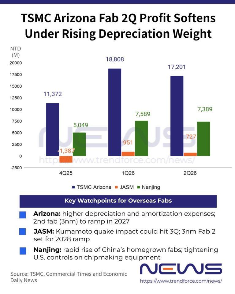
  As TSMC continues expanding its U.S. footprint, comments from Cliff Hou, TSMC Senior Vice President and Deputy Co-COO, have caught industry attention. According to Commercial Times, Hou said at the 2026 SelectUSA Investment Summit that the company “is prepared for growth from any new business opportunities,” remarks the market has interpreted as signaling potential further expansion of TSMC’s U.S. investments. TSMC’s total U.S. investment currently stands at US$165 billion.  Commercial Times notes that supply chain developments show chip equipment suppliers have also begun establishing U.S. subsidiaries to support TSMC. Industry sources added that TSMC’s total U.S. investment could reach as much as US$250 billion, with the company expected to replicate the Hsinchu Science Park cluster model in Phoenix.  Meanwhile, Economic Daily News reported that TSMC’s first Arizona fab entered mass production in 4Q24, while its second fab has already been completed and is expected to begin 3nm mass production in the second half of 2027. TSMC previously said construction of its third Arizona fab is already underway, while permits are being sought for a fourth fab and its first advanced packaging facility in the state. The report also noted that TSMC has acquired a second large parcel of land near its existing Arizona site to support future expansion plans.  Although TSMC’s U.S. fabs are more costly, capacity remains in strong demand, with previous reports indicating that customers had already reserved capacity at all four Arizona fabs, as noted by Economic Daily News. Institutional investors said that, for process technologies below 2nm, TSMC’s related capacity ratio between Taiwan and the U.S. is expected to reach roughly 7:3 by 2030.  TSMC Reshapes Board Amid Global Expansion  In addition, TSMC has also recently adjusted its board structure. According to Commercial Times, the company plans to revise its corporate charter by increasing the number of board seats from the current seven to ten directors to nine to twelve, with the proposal set to be discussed at the shareholders’ meeting on June 4.  The move reflects TSMC’s response to the rapidly changing global business environment and is intended to provide greater flexibility in recruiting directors from diverse professional backgrounds, the report said. It also noted that, as TSMC rapidly expands overseas and continues increasing its U.S. investments, the board will need more members with expertise in international supply chains, geopolitics, and U.S. policy.
2026-05-07 13:22 reading:775
  • Week of hot material
  • Material in short supply seckilling
model brand Quote
TL431ACLPR Texas Instruments
CDZVT2R20B ROHM Semiconductor
MC33074DR2G onsemi
RB751G-40T2R ROHM Semiconductor
BD71847AMWV-E2 ROHM Semiconductor
model brand To snap up
TPS63050YFFR Texas Instruments
ESR03EZPJ151 ROHM Semiconductor
BP3621 ROHM Semiconductor
IPZ40N04S5L4R8ATMA1 Infineon Technologies
STM32F429IGT6 STMicroelectronics
BU33JA2MNVX-CTL ROHM Semiconductor
Hot labels
ROHM
IC
Averlogic
Intel
Samsung
IoT
AI
Sensor
Chip
About us

Qr code of ameya360 official account

Identify TWO-DIMENSIONAL code, you can pay attention to

AMEYA360 weixin Service Account AMEYA360 weixin Service Account
AMEYA360 mall (www.ameya360.com) was launched in 2011. Now there are more than 3,500 high-quality suppliers, including 6 million product model data, and more than 1 million component stocks for purchase. Products cover MCU+ memory + power chip +IGBT+MOS tube + op amp + RF Bluetooth + sensor + resistor capacitance inductor + connector and other fields. main business of platform covers spot sales of electronic components, BOM distribution and product supporting materials, providing one-stop purchasing and sales services for our customers.

Please enter the verification code in the image below:

verification code