Unlocking Compound Semiconductors’ Economy-driving Potential
Silicon-based semiconductors and advances in computing technology have transformed our world within a short time frame. Nevertheless, we have now reached the limit of where silicon alone can take us, and innovative approaches are required for enabling the necessary advances in our digital lives.
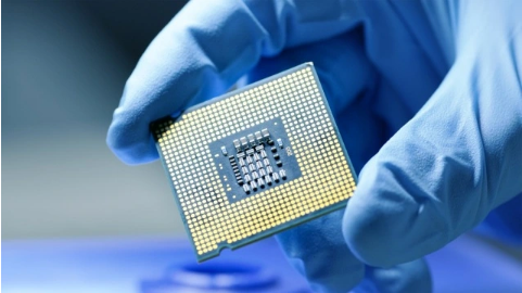
Our collective experience with the Covid-19 pandemic has demonstrated beyond a doubt that being connected is no longer optional. Fully realizing our individual roles in this emergent, interconnected society requires us to participate via our smart devices over increasingly powerful and intertwined networks.
New technologies ranging from the internet of things, Industry 4.0, and 5G/6G to electric/autonomous vehicles and augmented reality are placing unprecedented demands on incumbent semiconductors. Rising performance requirements leave traditional silicon semiconductors unable to address the challenges.
What, then, is the solution?
A way forward is available at the level of the semiconductor materials themselves: We must look beyond silicon. And there is a group of complementary semiconductor materials that can provide the opportunity to reach where silicon cannot.
Compound semiconductors, meaning those formed from two or more elements, include materials such as gallium nitride, gallium arsenide, and indium phosphide. These semiconductors are already powering many of the technologies on which our interconnected world relies. At the same time, their adoption is rapidly accelerating (growing at double the rate of silicon), and they are becoming mainstream in power electronics, sensing, connectivity, and advanced display applications.
But the growth story does not stop there. To achieve the next wave of innovation, engineers are marrying compound semiconductors with silicon to deliver a new generation of products that will be highly disruptive in terms of the performance attributes they offer, and at a scale that will enable the mass adoption of compound semiconductors.
The growth of compound semiconductors is enabled by epitaxy, the fundamental production process used to architect atomically engineered structures from which chip companies build electronic and optoelectronic devices. By selecting the right compounds and precisely controlling how the materials are deposited on a substrate, epitaxial-wafer producers have at their disposal a unique materials “toolset” that lets them tailor wafers to enable a wide variety of device types, from power amplifiers to sensors to lasers. The level of customization that epitaxy enables is unrivaled; hence, it is the key building block of the compound-semiconductor ecosystem.
The silicon industry and its foundries have built their success upon increasingly advanced lithography techniques, mastering successive process node generations and thereby producing progressively smaller transistor technologies — 5 nm, 2 nm, and so on.
Epitaxy is to compound semiconductors what lithography is to silicon. Epitaxy thus will be central to our efforts to move beyond traditional feature scaling based on Moore’s Law.
But how does one go about turning the potential of compound semiconductors into reality — and educating an industry that is accustomed to decades of reliance on silicon-based solutions? Simply put, we need open-access foundries to start producing state-of-the-art compound semiconductors.
By way of analogy, compare Intel with TSMC in the silicon space. How many designs per month does Intel work on? One or two? Half a dozen? Now consider TSMC, which is constantly adapting its processes to various designs, forcing it to learn, adapt, and improve continuously. These “best practices” benefit everyone in the chain, from the foundry all the way to the end user.
The same situation manifests itself in the compound-semiconductor segment. Some vertically integrated chipmakers are convinced that it is optimal to produce their epitaxy in-house. However, they can never learn as fast or be as agile as an open-access foundry that is constantly collaborating with multiple customers on multiple designs. This process of building experience and knowledge gives the open-access foundry model a significant edge in the innovation race.
Further, the environmental aspects of chip manufacture can no longer be ignored. The semiconductor industry must be “carbon responsible” and minimize the lifetime impact of its materials and processes. Resources can no longer be viewed as infinite. Energy consumption has consequences. The semiconductor industry must find a way to build a digital, interconnected world that is compatible with the global push toward zero net emissions. Advanced compound-semiconductor materials are enabling the industry to innovate, and thanks to their well-documented performance and efficiency attributes versus silicon, compound semiconductors provide a key building block along the path to net zero.
I was speaking recently with several key figures from the silicon industry who echoed these trends. They increasingly recognize the importance of compound semiconductors and acknowledge the strategic importance of epitaxy. In particular, there is a recognition of the enablement that compound semiconductors provide to the silicon industry.
As a result, the silicon- and compound-semiconductor advancements are no longer separate pursuits; rather, the two industries are more significantly collaborating to deliver disruptive technologies at scale. Epitaxy plays a critical role in this work.
Semiconductors are vital to the world economy. And with an ever-increasing focus on energy efficiency and ubiquitous connectivity, compound semiconductors are poised to deliver the next-generation technology solutions that silicon simply cannot.
在线留言询价
- 一周热料
- 紧缺物料秒杀
| 型号 | 品牌 | 询价 |
|---|---|---|
| CDZVT2R20B | ROHM Semiconductor | |
| RB751G-40T2R | ROHM Semiconductor | |
| BD71847AMWV-E2 | ROHM Semiconductor | |
| TL431ACLPR | Texas Instruments | |
| MC33074DR2G | onsemi |
| 型号 | 品牌 | 抢购 |
|---|---|---|
| STM32F429IGT6 | STMicroelectronics | |
| BP3621 | ROHM Semiconductor | |
| BU33JA2MNVX-CTL | ROHM Semiconductor | |
| ESR03EZPJ151 | ROHM Semiconductor | |
| IPZ40N04S5L4R8ATMA1 | Infineon Technologies | |
| TPS63050YFFR | Texas Instruments |
- 周排行榜
- 月排行榜
AMEYA360公众号二维码
识别二维码,即可关注


