New Issues In Advanced Packaging
Advanced packaging is gaining in popularity as the cost and complexity of integrating everything onto a planar SoC becomes more difficult and costly at each new node, but ensuring that these packaged die function properly and yield sufficiently isn’t so simple.
There are a number of factors that are tilting more of the the semiconductor industry toward advanced packaging. Among them:
SoC interconnects and wires are not scaling at the same rate as transistors.
Costs of designing and manufacturing chips at each new node are skyrocketing.
Resistance and capacitance are increasing at each new node, along with heat and various types of noise.
“Moore’s Law has served us extremely well so far, but there is a growing challenge of interconnect delays,” said Annapoorna Krishnaswamy, product marketing manager for the semiconductor business unit atANSYS. “The transistors are scaling and the delays are shrinking, but the interconnect is becoming a very big bottleneck.”
These and other issues are driving many chipmakers to seriously consider advanced packaging options, including 2.5D, 3D-ICs, various flavors of fan-outs, and system-in-package.
“The cost to fab is so much higher today, but with 3D-IC and advanced packaging technologies that cost can be mitigated,” Krishnaswamy said. “You can bring down the cost by integrating two chips within the same package. And with a shorter distance of communication, the time it takes for a signal to travel from one chip to another can be less than the time it takes for a signal to travel from one end to another on a big chip at an advanced technology node.”
There is widespread agreement on that subject. “Packaging technology is becoming real, whether it’s side-by-side or stacked using TSVs or interposers,” said Navraj Nandra, senior director of marketing for the DesignWare Analog and MSIP Solutions Group at Synopsys. “And the packaging costs are worthwhile developing because products without advanced packaging are crazy expensive.”
Advanced packaging also can reduce the amount of power needed to drive those signals, because the interconnects are wider and the distances are shorter. And it makes heterogeneous integration much simpler in some respects, because such issues as heat, electromagnetic interference, and power noise can be dealt with at the floor-planning stage.
There is no shortage of examples. Apple’s A-10 processor is a case in point. So are network processors from Cisco and Huawei, and various GPUs and AI architectures. Today, all of the top semiconductor companies have designs in development based on some form of advanced packaging. But as many of them have discovered, this isn’t as easy as it sounds.
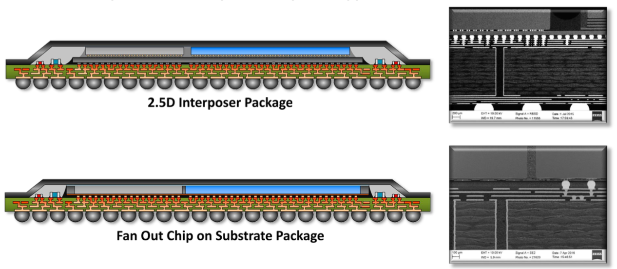
Fig. 1: The shape of things to come — fan-out chip on substrate. Source: ASE
“If it works, it can do great things,” said Raymond Nijssen, vice president of systems engineering at Achronix. “But it’s not a panacea. You have to decide how much memory to pair with a CPU, and that’s difficult to change because that memory is pre-packaged with the chip.”
He said that data rates for some solutions can be very high, but getting this wrong also can be expensive because it means throwing away multiple chips rather than one, including an expensive interposer layer. So yield is critical, and that is difficult to achieve with multiple die. “The Holy Grail is a module like a PCB, and we see a lot of interest in a more conventionalsystem-in-package with no interposer.”
Complexity multiplied
For now, however, interposers are a key part of advanced packaging. Increasingly, so are stacked die on top of interposers or some other substrate, in the form of pillars. And to understand just how complex this gets, picture three-die stacks atop a silicon interposer with eight pillars, for a total of 24 chips plus the interposer.
“If you want to check for power integrity [on a design like this], where each three-die stack is composed of either three SoC die, or two SoC die with one memory die, you may want to include everything in that simulation,” said Norman Chang, chief technologist at Ansys. “But in terms of capacity, that would be impossible.”
With a single three-die stack on top of a silicon interposer, the power integrity simulation is no problem, he said. “We can do the extraction for every die, including the TSV from the die to the silicon interposer, along with the internal TSVs from the bottom die to the interposer, from the bottom die to the middle die, and from the middle die to the top die. A simultaneous power integrity simulation can be done for that scenario.”
Simulating 24 chips requires a different approach. One option is to create a chip-power model for one of the stacks while condensing the other chips into a model. It’s critical that the middle die be checked for thermal integrity, and the best way to do that is to use thermal simulation. Here, a chip thermal model could be generated for each die, including the silicon interposer and the TSV in the detailed model of the thermal simulation, so the whole thermal simulation can be done for the 24 die on top of the silicon interposer, Chang explained.
Thermal-induced stress is a new issue that is cropping up for 2.5D and 3D designs. “If you look at the dielectric layer, which is the ELK (extra low-k) layer in the process, then you may suffer stress,” Chang said. “Solder joints and solder bumps traditionally had to be watched for stress, but this is a new, thermal-induced stress due to heat breaking down the materials. At higher temperatures, the stress is more severe.”
Knowing the neighbors
Another problem showing up in these advanced packages is the combination of electromagnetic interference (EMI), electromagnetic compatibility (EMC), electromagnetic susceptibility (EMS), and simultaneous switching output (SSO). EMI is the noise going out to the world, whereas EMS is the noise coming into the chip from outside. This is a new standard in the ADAS market because of noise through the direct power injection (DPI). In SSO, the signal must go through one chip to the other chip in the packaging. A specific simulation is needed for this as well.
Indeed, the over-arching challenge of 2.5D/3D heterogeneous design is that when one block is designed, it is not enough to verify the correctness of this one block by itself.
“We all know that it is important to consider what will happen to a block when integrated either with another block or with the entire chip around it,” according to Magdy Abidir, vice president of marketing at Helic. “There are many variations of this problem, but the wishful thinking of most people is that if I know what the neighbor is doing, and I try to understand the neighbor, it may mean keeping the neighbor away a bit. Why is this intuition true? Because it turned out for capacitive and resistive interactions that it is true. If you keep them away, the resistance is infinity while the capacitance is zero – so it works. But with inductance, it doesn’t because inductance has to do with loops. Current loops can exist in very big loops, which can make inductive magnetic effects between blocks.”
If, for example, there are two blocks and they are separated by a certain distance, when they are simulated, they may not interact with each other. But when they are put into a big chip, it may be a different story. As most SoCs contain a C-ring – which the manufacturer puts in for reliability purposes – even though it is not electrically connected, it is very large compared to the size of these two blocks, and therefore it is part of the physics.
“When you do the EM analysis, all of a sudden these two blocks start interfering with each other, and the problem is we have to be aware of the environment,” Abadir said. “We must be aware of what else exists on the chip even though it is not close by. This is a major challenge for a lot of engineering teams, and to SoC providers that cannot handle that kind of complexity. They really want to operate in a way that includes designing IP and putting it together, but that is not enough.”
Existing problem needs a new solution
While the need to be able to simulate heterogenous 2.5D and 3D designs has been a growing problem in the industry for at least the last five years, it is now reaching a critical stage. Today, it’s not uncommon for heterogenous designs to contain a half-dozen different technologies inside of a module, which contains upward of 20 ICs. This is due to the fact that for the optimum power, a specific manufacturing process may be used. Then for switching control, filters and switches, each may be manufactured with different processes, where the materials and process formulas are different.
“And that’s not mentioning the laminate board that they sit on and all of the SMTs,” said Michael Thompson, RF solutions architect in Cadence’sCustom IC & PCB Group. “The ability to handle multiple technologies in both simulation and layout – as well as to verify that what I laid out and how I connected these ICs together with the surface mount technologies actually reflect the schematic – has become a critical problem in the industry over the last few years.”
To accommodate this design paradigm, tool providers are beginning to support multiple process technologies in their simulation tools to handle a variety of different PDKs within the same tool. This also means they can be simulated together and laid out as different technologies. And this is just the beginning of the work in this vein. Tool vendors currently are working to augment tools further.
At the same time, existing tools are still being used. In fact, SPICE is used to do simulation at the chip level, and at the transistor level, Abidir noted. “But what you are feeding SPICE typically in the simulations are RC resistance and capacitive kind of extracted netlists of the chip. You are not seeing the impact of inductance. You’re not seeing the magnetic impact. And even if you have started to extract inductance for the long wires and interesting pieces, it is not very easy for a lot of the tools that are used to operating on smaller blocks to take their outputs, which is their EM models, and put it back into a chip environment. So there is still work to be done. [Many] tools don’t have a way to take that information back in.”
Another consideration is the fact that the low-power aspect of 2.5D and 3D designs makes circuitry a lot more sensitive because voltage levels are dropping, so noise obviously will impact it more. “Adding to the misery, there are reliability issues with thermal, where wires might get thinner,” he said. “As that happens, the inductance goes up, so the analysis that I have done might shift a bit because of the changing parameters, which may result in something that stops functioning six months later-or worse, something that didn’t fail starts missing bits. In a situation like autonomous driving, I’m assuming it looks like it’s doing the data analysis and forecasting the accident before it happens, but if the chip starts failing a little bit, there’s no telling what could happen.”
More complexity ahead
Looking ahead, Ansys’ Chang expects a number of designs with three-die stacks will show up this year containing pillars on silicon interposers. Most of those will have a mix-and-match, wafer-to-wafer die stack on top of a silicon interposer. This will translate to the use of additional advanced packaging technologies, including package-on-package and a number of other variations.
The result is that complexity will continue to increase, but now it will happen in multiple directions. Understanding the impact of all of these pieces on each other is a huge challenge, and it’s one that will continue to evolve as advanced packaging continues to gain ground as an alternative to planar scaling.
在线留言询价
- 一周热料
- 紧缺物料秒杀
| 型号 | 品牌 | 询价 |
|---|
| 型号 | 品牌 | 抢购 |
|---|
- 周排行榜
- 月排行榜
AMEYA360公众号二维码
识别二维码,即可关注

