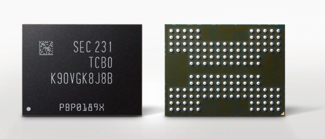
Samsung, Micron Battling for NAND Supremacy
Samsung Electronics and Micron Technology continue to fight for supremacy in the NAND market, with both companies recently announcing higher-density 3D NAND solutions—albeit with different nomenclatures.

Samsung has opted to focus on 3D NAND bit density with the introduction of its 1-terabit (Tb) triple-level–cell eighth-generation vertical NAND (V-NAND), which the company claims is the industry’s highest bit density. Meanwhile, Micron has opted to present its latest 3D NAND in term of layers, having announced its 232-layer 3D NAND mid-year in 2022.
Samsung’s eighth-gen V-NAND
SungHoi Hur, executive vice president of flash product and technology at Samsung, told EE Times during an interview that the company achieved high bit density through a Cell-on-Peri (COP) structure, which the company introduced with its seventh-generation V-NAND.
With a COP structure, a cell array area is placed above the peripheral. But even with a COP structure, part of the peripheral is placed outside of the cell, Hur said, meaning the cell array must be reduced along with the peripheral area below and next to the cell array to reduce chip size.
Samsung first introduced its vertically stacked V-NAND flash in 2013. “Since then, we have been developing disruptive technologies to reduce the area and height of cells and have accumulated a great deal of Samsung know-how,” Hur said.
That know-how includes Samsung’s high-aspect–ratio contact etching technology, which the company uses to reduce the area of the cell array. For the eighth-generation V-NAND, Samsung successfully minimized the area of all three parts from the previous generation to enable even more density, Hur added.
A specific challenge that Samsung aims to address is avoiding the cell-to-cell interference that normally occurs with scaling down if the mold of the cell unit gets slimmer for scaling. “To counteract that interference, we have identified possible tradeoffs in performance first; then we moved on to solving the fundamental problems,” Hur said.
He also noted that the purpose of Samsung’s solution was to develop an optimal operation scheme for minimizing interference during writing, applying a new material to the blocking layer in the cell to prevent electrons from bouncing out of the charge trap layer (CTL) due to voltage and improving the structure of the CTL.
Hur said reaching this milestone means overcoming a variety of hurdles. From a structural perspective, the molds could lean to one side more easily as the total stack height continues to grow. “As the cells become closer and smaller, we have to fight with decreasing cell current as well as interference among cells,” he said. Samsung is working to lower the total stack height by leveraging the support structure used in its seventh-generation V-NAND and the multi-hole technology while also exploring new solutions, including an innovative cell structure using new materials.
在线留言询价
- 一周热料
- 紧缺物料秒杀
| 型号 | 品牌 | 询价 |
|---|
| 型号 | 品牌 | 抢购 |
|---|
- 周排行榜
- 月排行榜
AMEYA360公众号二维码
识别二维码,即可关注

